
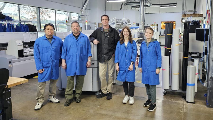
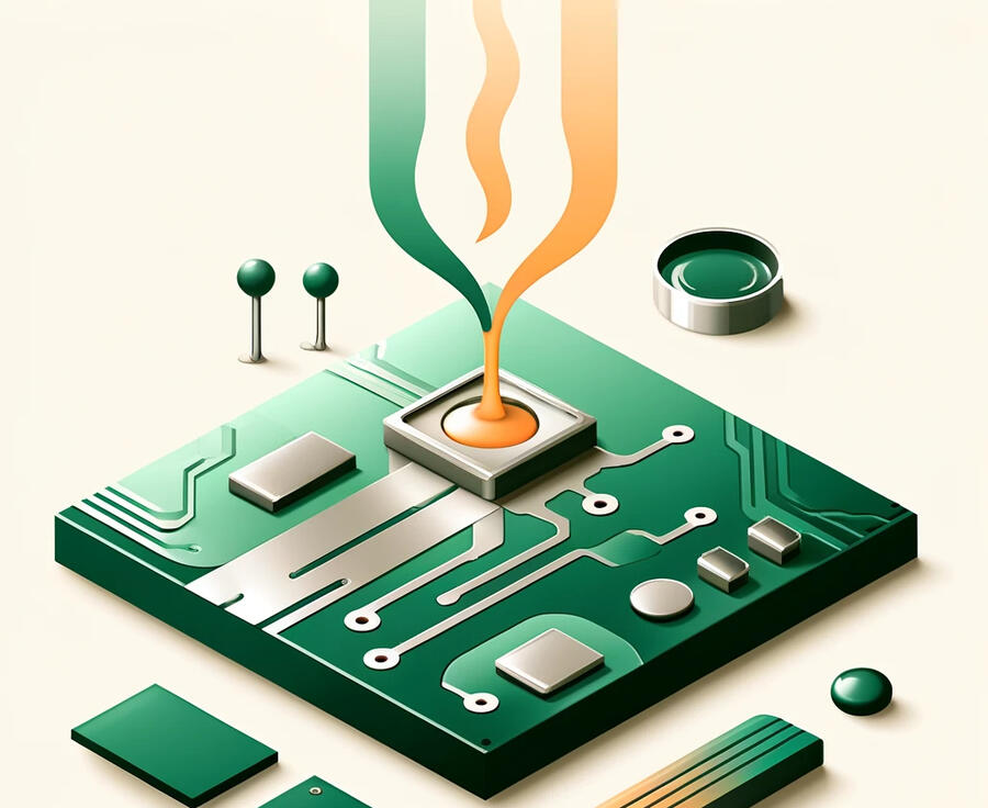
About Us
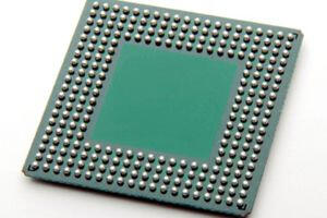
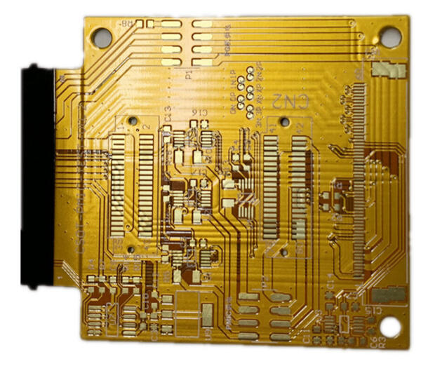
Sacramento PCB Assembly offers a comprehensive printed circuit board assembly service that covers every aspect of the process, from initial part procurement to final shipping. Utilizing a blend of cutting-edge technology and skilled craftsmanship, we ensure precision and quality at every step. The service includes meticulous planning based on an approved Bill of Materials (BOM), precise solder paste application, automated and manual component placement, and a variety of soldering methods tailored to each project's unique requirements. Advanced inspection techniques, such as [3D Automated Optical Inspection AOI and X-Ray technology, are employed to guarantee the highest quality standards. The end result is a meticulously assembled PCB, cleaned and packaged with industry-standard materials, ready for immediate integration into your projects. We are ISO 9001 and 13485 certified.
Services
Our expertise extends to a range of specialized services:•Custom Printed Circuit Board Design: Tailored to your specific needs, ensuring high performance and reliability.•Precision PCB Assembly: Meticulous assembly processes to bring your designs to life with exceptional accuracy.•Advanced X-Ray Inspection: Utilizing cutting-edge technology to ensure the highest quality and integrity of your PCBs.PCB Repair: Our technicians can do PCB repair on a case by case basis. Contact us for a consultation.


Testimonials

Working with this Sac PCB Assembly has been an exceptionally smooth experience. They have clearly invested heavily in their PCB equipment and have a talented team dedicated to designing and manufacturing high-quality products. Throughout my project, their communication was commendable. They consistently kept me informed with detailed updates at each stage, ensuring that I was always in the loop. It never felt like I was taking a risk and was a great experience overall. I look forward to working with them in the future.-Manny Bains

Photon Ink has been working with Sacramento PCB Assembly for several years and their service is unmatched. Myles and his team are easy to work with, flexible and quick to respond. They strive to please their customers and never cease to meet our needs and expectations.
-Kristie Brown

We developed a breadbot to make fresh bread in stores. We had issues with our old control system, so went to Sam and the team to design and build a custom PCB system and software package. They designed and built a perfect solution from pcb to cloud. We are very happy with the final product and have had almost zero issues in the field with the boards. We work with hundreds of suppliers and Sam and team are by far the best. They understand their domain and are great to work with. I would highly recommend.
-Eric Wilkinson


FAQs
What's your process?
Our PCB assembly process is outlined here.Are you ISO certified?"
Yes, we are ISO 9001 and 13485 certified.What are some of the equipment you use?
A list of the equipment we use for our PCB Assembly can be found here.Do you offer X-Ray inspection?
Yes we do. We employ 2D and 3D imaging technologies to accurately identify assembly defects and perform in-depth analysis on PCBs, ensuring swift and consistent inspections powered by YXLON Cheetah EVO technology.Do you perform work to IPC standards?
Yes, our work is performed to IPC standards.What's your contact information?
Our phone number is (916) 692-9706 or you can drop us a message hereWhat are your traceability capabilities?
A description of our advanced traceability capabilities can be found hereWhere are you located?
Our address is
5175 Hillsdale Cir Suite 150, El Dorado Hills, CA 95762Can we take a tour of your facility?
Yes, call us at (916) 692-9706 to arrange a tour.

Our Process
1. PROCUREMENT AND PLANNING

Starting a PCB project kicks off with acquiring the necessary parts. After the project's specifications are set, we source the components and create a Bill of Materials (BOM), detailing each component, its manufacturer, and delivery information. Once you approve the BOM, we order the parts. Your project officially starts when these parts arrive. Upon arrival, we categorize the parts by project, scan them into our system, and track them during the PCB assembly. This meticulous process guarantees precise component placement and allows us to pinpoint and resolve any issues efficiently.
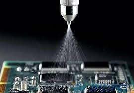
2. SOLDER PASTE
Before attaching components to a PCB, solder paste must be precisely applied to specific areas, primarily the component pads. This paste is a mixture of metal alloy powder and flux, a putty-like substance, and applying the right amount is critical to avoid misalignments or poor connections. There are two methods for this: using a solder screen or a jet printer. The solder screen, created during the board design process, has holes aligned with the board's solder-required areas. Paste is spread over the screen and then scraped through the holes to the board. In contrast, a jet printer, which is like a conventional printer, receives coordinates for where to apply paste and precisely deposits it in tiny dots on the component pads. While jet printers are more accurate and reduce solder waste, they are not as quick as the screen printing technique.
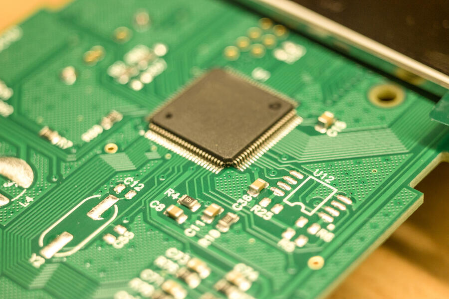
3. COMPONENT PLACEMENT
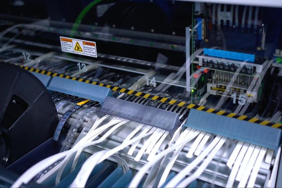
Following the solder paste application, boards now termed 'wet boards' are ready for component placement. While some larger or through-hole components are manually placed, most components are positioned onto the board using pick and place machines. These machines function as their name implies: they pick up each component and place it accurately on the board. Components are loaded into the machine in reels, and using specialized software, the precise location and orientation of each part are programmed. During operation, one or multiple heads of the machine pick up the components, align them as per the design specifications, and place them onto the wet solder. This holds the components temporarily in place until they are permanently affixed through the soldering process.
4. SOLDERING
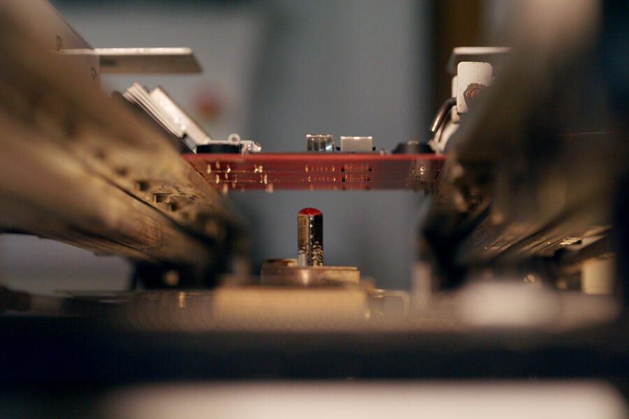
After a board is fully assembled with components, the next step is to melt the solder to permanently attach these parts to the board. This process varies based on the component's size, placement, and type, and can be done through hand soldering, reflow ovens, or selective soldering methods. In reflow ovens, boards are moved on conveyor belts through various heating and cooling zones. Technicians tailor the conveyor's speed and the temperature in each zone to create specific time-temperature profiles, ensuring the solder melts as needed for each specific project. Selective soldering, on the other hand, involves a nozzle guided by a set of coordinates to apply a targeted molten solder fountain to unsoldered components. This method is particularly useful for parts that need soldering after initial reflow oven processing, requiring precision to avoid damaging adjacent, already soldered parts. If selective soldering isn't suitable, our skilled technicians undertake hand soldering, using state-of-the-art Metcal soldering equipment, to ensure the highest quality in PCB assembly.
5. INSPECTION
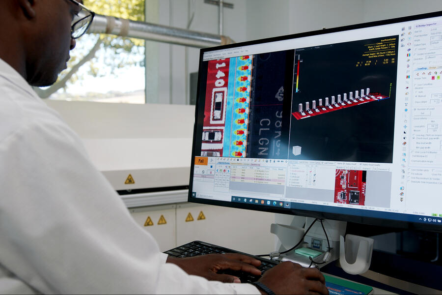
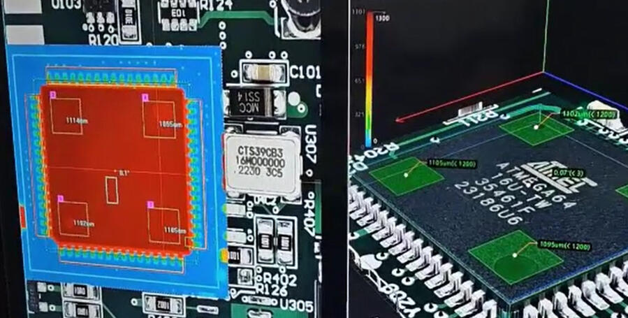
Inspections in PCB production are integral and occur at multiple stages, including key Automated Optical Inspection (AOI) checks on wet boards for solder paste. However, the bulk of inspections are conducted post-completion, as manual checking of surface mount boards with extensive components is impractical. Instead, 3D AOI and X-Ray technologies are utilized for thorough analysis. AOI uses intense light flashes to reveal imperfections and read part numbers, quickly assessing each component's presence, location, and orientation, and detecting issues like bent or lifted leads with its volumetric height measurement. X-Ray inspection, essential for uncovering internal defects and examining parts hidden by others, employs non-destructive techniques. While 2D X-Ray excels in individual board or component examination, particularly for void analysis, 3D X-Ray takes thousands of images to reconstruct detailed views of whole or parts of boards and components, ensuring even the smallest elements are meticulously inspected.
6. CLEANING, PACKING, AND SHIPPING
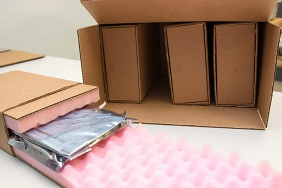
Once all required components are sourced, soldered onto the boards, and the boards have successfully passed all necessary inspections, they are nearly set for dispatch. The final step involves a gentle cleaning process to eliminate any residual solder paste, glue, or other substances acquired during assembly. After this, the boards are meticulously packaged using industry-standard, antistatic materials, ensuring their safe and secure delivery to the customer.

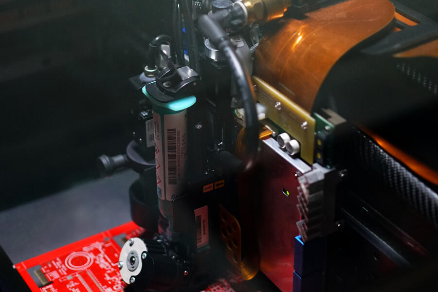
Our Equipment
Sacramento PCB Assembly utilizes an array of top-tier machinery to facilitate both the assembly and quality inspection of each project.
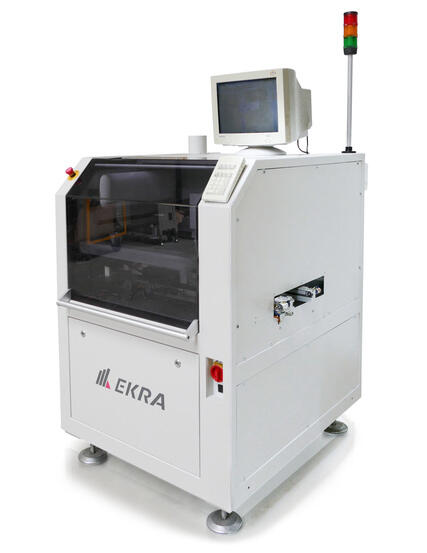
Asys Group Ekra X4
The EKRA X4, by ASYS Group, is a high-precision automatic screen and stencil printer tailored for diverse production demands within the electronics industry, with a notable ease of use and flexibility. It's engineered for precise application of solder paste and/or glue onto substrates like PCBs, ceramics, or glass, within a printing area of 460 x 460 mm. The EKRA X4 boasts quick reconfiguration, facilitated by a user-friendly interface and simple programming, alongside a patented optical positioning system for accurate material application. Its robust construction ensures stability, while specifications like a power rating of 230V 50/60Hz 2.0 kW 16 Amp, two pneumatically driven print heads, and a quick product changeover in less than 5 minutes underscore its efficiency and user-centric design. Additional features like variable stencil pickup, optical solder paste detection, and Grid-Lock PCB support enhance its functionality, making it a reliable choice for high-efficiency, precise printing in the electronics industry.
Mycronic MY600 Jet Printer
The Mycronic MY600 Jet Printer is a cutting-edge device designed for stencil-free solder paste application on PCBs, optimizing both speed and precision in the process. With the ability to dispense over one million dots of solder paste per hour, it achieves a 50% increase in throughput compared to earlier models. The MY600 operates with micrometer accuracy, even at high speeds, handling complex boards efficiently by optimizing paste volume for each solder joint using non-contact technology. Its sophisticated system calculates the trajectory of each dot in real-time, akin to a plane determining when to drop a bomb, thus allowing continuous printing at a pace of 600 dots every second without pause, significantly accelerating the PCB assembly process while ensuring high-quality solder joints on challenging circuit boards and components.
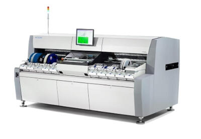
Mycronic MY300ex
The Mycronic MY300EX is a cutting-edge device designed for stencil-free solder paste application on PCBs, optimizing both speed and precision in the process. With the ability to dispense over one million dots of solder paste per hour, it achieves a 50% increase in throughput compared to earlier models. The MY600 operates with micrometer accuracy, even at high speeds, handling complex boards efficiently by optimizing paste volume for each solder joint using non-contact technology. Its sophisticated system calculates the trajectory of each dot in real-time, thus allowing continuous printing at a pace of 600 dots every second without pause, significantly accelerating the PCB assembly process while ensuring high-quality solder joints on challenging circuit boards and components.
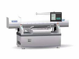
Mycronic MY9
The Mycronic MY9 is a distinguished pick-and-place machine tailored for efficient surface mount technology (SMT) assembly. Its core strength lies in precision placement, reducing material waste while maximizing production yields. Designed for speed, the MY9 accelerates component handling and placement rates without sacrificing accuracy, crucial for adhering to stringent production schedules. It showcases versatility in handling a broad spectrum of SMT components, making it apt for both standard and complex assembly tasks. The user-friendly interface simplifies operations, minimizing downtime and ensuring a swift learning curve in bustling production settings. An integrated automated vision system autonomously aligns and corrects component positions before placement, significantly lowering error margins and upholding consistent quality output. The MY9 is engineered for seamless integration with other assembly line machinery, promoting an efficient, synchronized production flow. Additionally, its expandable configurations allow it to adapt to evolving production demands, displaying a future-ready approach. With an eye on sustainability, the MY9 operates with energy efficiency and waste reduction at its core, aligning with modern sustainable manufacturing mandates. The functional prowess of the Mycronic MY9 makes it a robust, pragmatic choice for those keen on optimizing their SMT assembly processes.
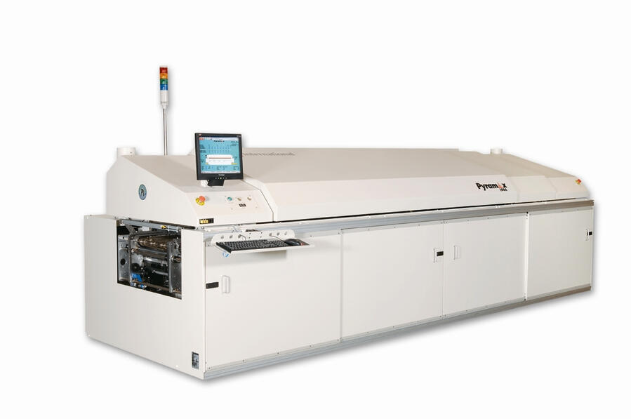
BTU International Pyramax 98
TheBTU International Pyramax 98 is a sophisticated forced convection lead-free reflow oven, designed to excel in high-demand manufacturing environments. It features 7 vertical heating zones with top and bottom heaters, ensuring precise temperature control throughout the solder reflow process, and a maximum temperature capacity of 350°C for high-temperature applications. Enhanced by the integration of the SuperM.O.L.E.® Gold 2 Thermal Profiler, the oven allows for the creation of precise, custom oven profiles, ensuring optimal performance tailored to specific needs. The unit also includes a dedicated cooling zone with two-speed control blowers, a combination of Pin-Chain and Centre Board Support Conveyor system, and an adjustable width conveyor setup, accommodating various board sizes and ensuring smooth material transit. Operating on a 208V or 440V, 3 Phase power supply, the Pyramax 98 stands as a reliable and versatile choice for a myriad of solder reflow requirements.
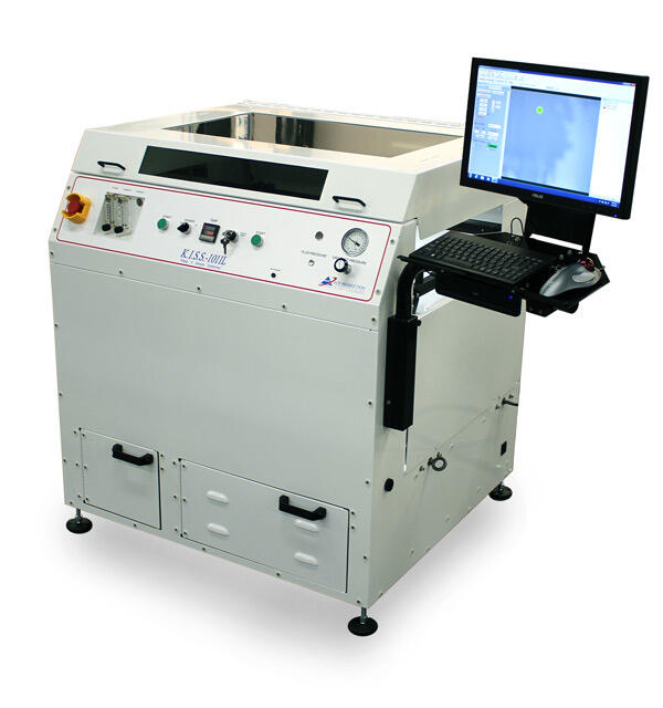
ACE KISS 101
The ACE KISS 101 is a selective soldering system adept at soldering through-hole components on Surface Mount Technology (SMT) boards, especially beneficial when the components are near adjacent parts. It curtails manual soldering challenges and labor costs through an automated molten solder delivery system, further enriched by a range of programmable features allowing precise control over process parameters such as flux deposition, immersion depths, and solder temperature. With its high throughput, it's capable of outperforming multiple operators, while also offering an array of standard and custom nozzles for varied soldering needs. The system, known for its ruggedness, supports lead-free solder, making it suitable for low to medium volume assembly operations. The KISS 101B variant comes with ACE KISS Teach 2.0 software for enhanced process control and monitoring, presented as a low-cost, user-friendly, free-standing, and CE-compatible model, signifying its compliance with crucial safety and performance standards, ideal for quick-turn rework or light assembly facilities.
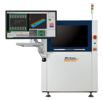
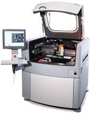
Mirtec MV-6 OMNI
The Mirtec MV-6 OMNI is engineered to boost productivity in the inspection of Printed Circuit Board Assemblies (PCBA) through its high-speed, high-performance 3D Automatic Optical Inspection (AOI) capabilities. Key features include a 15 Mega Pixel CoaXPress Camera Technology for detailed imaging, an advanced Eight Phase Color Lighting System for enhanced defect detection, and a 10 Micron/Pixel Precision Telecentric Compound Lens Design for accurate imaging. Additionally, it boasts an Integrated Ten Mega Pixel SIDE-VIEWER® Camera System for comprehensive inspection from different angles, Non-Blind Spot Digital 8 Projection Moiré 3D Inspection Technology for precise component and micro crack detection, a Precision Closed Loop AC Servo Drive Motor System for exact operation, and user-friendly programming and operation functionality, making it a reliable and robust tool for thorough PCBA inspection.
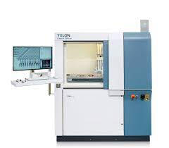
YXLON Cheetah Evo
The YXLON Cheetah EVO is a robust inspection system optimized for detailed examination, particularly in electronics. Its large flat-panel detectors enhance the field of view by up to 50%, expediting automated processes. With high-resolution inspection capabilities, it employs dynamic image enhancing filters like eHDR for refined imagery. The system harbors advanced technologies like FeinFocus X-ray tube and High Power Target technology for superior 2D and 3D imaging. It's ready for Industry 4.0, featuring integrated workflows and automated software solutions like the Comet Yxlon FF CT and YXLON ProLoop for real-time reporting and faster visualization. The intuitive workflow facilitates easy programming of automated procedures, and its flexibility is showcased in three models catering to varied inspection needs, demonstrating its adaptability in modern inspection scenarios.

Precision with Advanced Traceability
At Sacramento PCB Assembly, we're revolutionizing the electronics manufacturing industry with our state-of-the-art traceability capabilities. Our commitment to precision and reliability is evident in every Printed Circuit Boards (PCBs) we assemble. Let's explore how our sophisticated traceability methods are setting new standards in PCB assembly.Enhanced Batching and Component VerificationOur journey towards unparalleled precision begins with an innovative batching process. As components arrive to be mounted on circuit boards, they're assigned a unique batch number, and a photograph of the component package is taken, displaying part numbers. This system links each batch to its specific purchase order and receipt from our trusted authorized distributors, ensuring complete traceability for every component we use.Unique PCB Serialization for Complete TraceabilityAt the heart of our traceability system lies the unique serialization of each PCB. Every board we produce at Sacramento PCB Assembly is given a distinct serial number, creating a traceable identity that is essential for maintaining high standards of accountability and quality.Automated Component Placement and DocumentationUtilizing the latest in automated technology, our equipment meticulously documents and stores the batch number for every component placed on each uniquely serialized PCB. This extends to measuring resistor and capacitor values before placement, allowing for actual values to be documented and reviewed in the future. This attention to detail ensures that every component on each PCB is precisely traceable.The Traveler System: A Testament to Our Commitment to QualityOur traveler system is a testament to our dedication to quality. It begins with a cover sheet listing the primary specifications for PCB assembly, including IPC Class adherence and RoHS or ITAR compliance. Every process in the PCB assembly is documented, with our skilled technicians signing and dating each step upon completion. These documents are scanned and stored in our database, offering a detailed and retrievable record of the entire assembly process.Advanced AOI Inspection for Flawless Quality AssuranceOur Automated Optical Inspection (AOI) system is a cornerstone of our quality assurance process. It not only captures images of each inspected PCB linked to its unique serial number but also uses optical character recognition to validate branding marks on ICs against component datasheets. This meticulous inspection ensures that only the correct components are used, upholding our commitment to flawless quality.Comprehensive Traceability: The Sacramento PCB Assembly AdvantageTo summarize the robustness of our system: Every component, ordered according to the Bill of Materials, is traced right from its batch number to its placement on the PCB. Our advanced equipment precisely places each component, recording all necessary details. Post-assembly, our AOI system thoroughly inspects and documents each component on the finished boards.This comprehensive traceability enables us at Sacramento PCB Assembly to provide detailed information about any component on a PCB, even if it was assembled years ago. Whether it's retrieving images of the component batch, purchase history, or its exact placement on the PCB, our system ensures that this information is just a query away.In conclusion, the advanced traceability capabilities at Sacramento PCB Assembly epitomize our dedication to delivering precision, reliability, and transparency in electronics manufacturing. By meticulously tracking every component and process, we provide our clients with the highest quality standards and peace of mind in their electronics manufacturing endeavors.
Blog

Ansync Labs Awarded Ecosystem Builder Award
Ansync Labs, the parent company of Sacramento PCB Assembly, has been recognized with the Ecosystem Builder Award at the GFX2023 Backyard Awards. This award is a tribute to organizations that dedicate resources, time, and expertise towards nurturing a flourishing entrepreneurial ecosystem for the benefit of founders and the wider regional community.Located in Northern California, Ansync Labs is a design for manufacture firm that adopts a multidisciplinary approach towards solution development, iteration, and product realization. Our team of electrical, software, and mechanical engineers, backed by an in-house machine shop and electronics assembly line, strives to contribute meaningfully to practical solution delivery. Our endeavors span across motors and automation, medical, and IoT devices, areas where we hope to make a positive impact.The GFX2023 Backyard Awards, facilitated by Growth Factory and supported by Stoel Rives, is a heartfelt initiative that acknowledges the significant work being done locally, particularly in the Greater Sacramento area. Amid a world often focused on global events, this event brings attention to the meaningful contributions occurring right within our community.Being honored with the Ecosystem Builder Award is a gentle reminder of the importance of our mission to support the entrepreneurial ecosystem of the region. This recognition is not a destination but a milestone that encourages us to continue our efforts with renewed vigor. It also serves as a modest example for other organizations, showcasing the potential for positive contributions to our local entrepreneurial environment. While we are thankful for this recognition, it further motivates us to continue our work, fostering a nurturing environment for entrepreneurship within our community, and contributing towards a brighter and more innovative future for all.
Blog
Getting It Built: Moving from Prototype to Production
In the bustling world of startups, taking a product from prototype to production is often seen as a daunting task. It's a convoluted process that involves a slew of variables, from securing funding to managing supply chains. Sam Miller, the founder of Ansync Labs, presented to Startup Grind Sacramento on [Getting It Built: Moving from Prototype to Production. Here's what he covered:The Challenge of Funding and MarketingAccording to Miller, startups often find themselves in a conundrum when it comes to securing sufficient funding. They either miscalculate the required budget or run out of resources before reaching the end goal. The solution? A meticulously designed financial plan that incorporates room for setbacks and pivots.As Miller noted, marketing isn't a secondary concern; it's integral to the product development process. You need to be clear about who your target customers are and how you're going to reach them, ensuring your marketing and sales strategies are airtight.Vendor Relationships: The Unseen BackboneOne of the vital aspects Miller stressed was the importance of establishing strong vendor relationships. Whether it's custom screws or advanced electronic components, finding the right vendor can be a game-changer. He advocated for a strategy that cultivates long-term, mutually beneficial relationships with vendors. This involves diligent research, vetting, and ongoing communication to ensure quality and reliability.The Balancing Act: Overseas vs. Domestic ProductionShould you manufacture your product domestically or offshore it overseas? According to Miller, the answer lies in a balance. High labor portions of your product can be produced more cost-effectively overseas, while more complex or sensitive components might be best manufactured domestically. The key is to carefully consider factors like shipping costs, tariffs, and quality control, thereby striking a balance that aligns with your production goals and values.The Importance of Tolerances and SpecificationsIn Miller's view, a detailed and accurate specification sheet is worth its weight in gold. By providing vendors with precise tolerances and requirements, you minimize misunderstandings, reduce costly errors, and ensure the final product meets quality standards. It's about not leaving room for assumptions, thus preventing future headaches.The Concept of a 'Supply Funnel'Miller introduced the notion of a 'Supply Funnel,' explaining that products are built in stages, moving from individual components to sub-assemblies and finally, to the finished product. Effective management of this funnel can lead to streamlined operations and a faster time-to-market. The strategy here is to identify which components can be outsourced, how they will be assembled, and where the final product will be made, optimizing each step of the supply funnel for efficiency and cost-effectiveness.In conclusion, transitioning from a prototype to a production-level product is no small feat. But with clear planning, strong vendor partnerships, and a well-calibrated balance between domestic and overseas production, startups can navigate this complex journey more efficiently. As Sam Miller effectively demonstrated, it's not just about getting it built; it's about getting it built right.
Blog

A talk with Myles Pilkay, PCB Assembly Manager at Ansync LabsMyles Pilkay has been leading the PCB Assembly team at Ansync Labs since August 2015 (Sacramento PCB Assembly is a part of Ansync Labs), overseeing the production of complex circuit board assemblies with a strong emphasis on quality and efficiency. After earning a B.S. in General Chemistry from Sacramento State University in June 2015, he pursued opportunities in manufacturing, drawn by his passion for hands-on work and problem-solving. Throughout his career, he has collaborated with both internal teams and external partners to drive continuous improvement and innovation.Q: Can you tell us about the Sacramento PCB Assembly? When was the company formed and what type of PCB Assembly services do you provide?Myles: Founded in 2001 by Sam Miller as a subsidiary of Ansync Labs, Sacramento PCB Assembly (SPCBA) has evolved into a premier assembly house at the forefront of innovation. With a foundation rooted in expertise, we boast advanced machinery, a highly skilled IPC-certified production team, and a relentless commitment to quality.From in-house procurement and project management to electrical engineering and PCB layout, SPCBA offers comprehensive solutions under one roof. Our strategic location, cutting-edge testing equipment, and specialized capabilities enable us to excel in short-run, high-complexity, and fast-turnaround PCB assembly projects.Whether you need precision engineering or agile production, SPCBA is your trusted partner for mission-critical PCB assembly needs.Q: How do you differentiate your PCB Assembly Services from other PCB companies?Myles: At Sacramento PCB Assembly, our commitment to quality is unmatched, and it begins with our rigorous testing and QA procedures. Every assembly is subjected to our state-of-the-art Automated 3D Optical Inspection System (AOI), which ensures precise component placement, accurate connection part number verification, and optimal solder volume.For even greater assurance, our Yxlon live X-Ray, laminography and CT system provides a significant advantage. This advanced technology enables us to confirm solder volume and connectivity for bottom termination components like BGA and LGA packages. It also identifies solder voids and uncovers potential internal PCB defects, delivering unparalleled quality control.Another key differentiator is our in-house Electrical Engineering and Logistics team. This multidisciplinary group provides expert guidance at every stage of your project—from parts procurement to design reviews and revisions. With SPCBA, you’ll have immediate answers and hands-on support to keep your project on track.Q: What industry/market segments do you cater to? Which segment is the largest for you?Myles: At Sacramento PCB Assembly, we pride ourselves on our versatility. Our projects span a wide range of industries, from automated car wash controllers to government-contracted assemblies. With such a broad scope, we don’t focus on a single “largest” segment. Instead, our business model is built on diversifying our customer base to ensure adaptability, resilience, and exceptional service for clients across all sectors.Q: Can you tell us about your facility? Do you assemble all orders in-house or do you outsource these to partners?Myles: Sacramento PCB Assembly operates within a 10,000 sq. ft. facility designed for precision and efficiency. Our space houses two dedicated assembly lines equipped with cutting-edge technology, including solder jet printers, Selective Solder for T/H components, Hydra head pick-and-place machines, reflow ovens, Automated 3D Optical Inspection (AOI) systems, and X-Ray capabilities.We take pride in maintaining clean, efficient work areas and an organized workflow that ensures every aspect of our operation is meticulously managed. From start to finish, all assemblies are processed in-house, allowing us to maintain full control over quality and timelines.Q: Do you test PCB Boards once they have been assembled? Can you tell us about the PCB Testing capabilities that you offer as part of the assembly process?Myles: At Sacramento PCB Assembly, we offer in-house PCB assembly testing for projects where it is warranted and a test procedure is in place. These procedures are typically defined by the end user and customized to meet the unique requirements of each project.Our testing capabilities cover a wide range of procedures, from simple power-on tests to advanced FPGA programming and testing in end-use applications. We also provide full functionality testing for various devices, meticulously following the end-user-defined procedures to ensure accuracy and performance.You gain a partner with SPCBA dedicated to delivering thorough, reliable testing that aligns with your project’s exact needs.Q: How does your team balance automation and manual craftsmanship in the assembly process to maintain high-quality standards?Myles: At Sacramento PCB Assembly, we understand that a successful assembly process requires a seamless balance between advanced automation and skilled manual craftsmanship. As technology evolves, PCBs continue to shrink, demanding levels of precision that exceed the capabilities of the human hand and eye. This is where our state-of-the-art automation steps in, delivering the accuracy and efficiency that modern assembly requires.Automation not only ensures precision but also significantly enhances efficiency. Tasks that might take a technician an entire day can be completed in just 20 minutes using our well-defined automated programs and cutting-edge equipment. However, while automation is a cornerstone of our operations, it’s not the whole story.In a perfect world, 100% of our assembly processes might be automated—but the "human" touch remains essential. From addressing intricate details to ensuring proper assembly, our skilled team provides the expertise and attention to detail necessary to meet our primary goal: delivering exceptional quality.Q: Do you offer Repair and Rework services? Can you explain your process for diagnosing and repairing faulty PCBs?Myles: While rework and repair services are not something we actively promote, Sacramento PCB Assembly is equipped to diagnose and repair faulty PCBs when necessary. Our top priority is always the boards assembled in-house at SPCBA, but we also welcome external PCBs for evaluation and repair.When it comes to fault diagnosis, our go-to method is advanced 2D and 3D X-Ray inspection. This cutting-edge technology allows us to identify issues that would otherwise go undetected, particularly with modern components like BGA, LGA, and QFN packages. These components often feature solder connections that are invisible under a microscope or through traditional AOI methods.Q: Who are your customers and where are they located? In terms of regions do you prefer to work with local or global customers? What is the current break up for you?Myles: At Sacramento PCB Assembly, we proudly serve a diverse customer base. While many of our clients are located here in California—making up approximately 70% of our business—we also work with customers across the United States, accounting for 25% of our projects. Additionally, we collaborate with a select group of international clients, representing the remaining 5% of our customer base.Q: How has 2024 been for you so far in terms of business growth?Myles: 2024 was an outstanding year for Sacramento PCB Assembly! We achieved a significant 33% increase in revenue and grew our customer base by an impressive 15–20%. This growth reflects the trust our clients place in us and our unwavering commitment to excellence.As we look ahead to 2025, the future is even brighter. We are forecasting an additional 50% growth in revenue, alongside another 15–20% expansion of our customer base. These projections are a testament to our team’s dedication, our industry-leading capabilities, and our ability to consistently deliver high-quality results.We’re excited to continue building on this momentum and achieving new milestones with our valued clients and partners.
Blog
What is Conformal Coating on a PCB?Conformal coating is a thin, protective layer applied to printed circuit boards (PCBs) to shield them from environmental damage. This coating acts as a barrier against moisture, dust, chemicals, and extreme temperatures, helping to prevent corrosion and extend the life of the board.The coating, which can be made from materials like acrylic, silicone, or polyurethane, conforms to the shape of the PCB and its components. By providing this layer of protection, conformal coating ensures the board continues to function properly, even in harsh environments like aerospace, automotive, and medical applications.In industries where reliability is key, conformal coating is an essential step in PCB manufacturing.
Blog
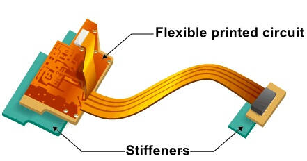
What Are PCB Stiffeners and Why Are They Important?Printed circuit boards (PCBs) are the backbone of modern devices, and as technology advances, flexible PCBs are becoming more popular due to their ability to fit into tight spaces. However, flexibility can sometimes be a disadvantage, especially when a board requires stability for mounting components or connectors. This is where PCB stiffeners come into play.What Are PCB Stiffeners?PCB stiffeners are non-electrical elements added to flexible PCBs to provide structural support. Made from materials like stainless steel, aluminum, or rigid laminates, stiffeners prevent bending or warping in critical areas. They are particularly useful in ensuring that components stay securely attached, maintaining reliable electrical connections and preventing damage during handling or operation.Why Are PCB Stiffeners Important?- Mechanical Support: Stiffeners add rigidity to sections of the board that need extra strength, particularly around connectors or mounting points.
- Ease of Assembly: A stiffer board is easier to handle during manufacturing and assembly, ensuring accurate placement of components.
- Improved Reliability: By preventing flexing in key areas, stiffeners help maintain the integrity of solder joints and electrical connections, reducing the risk of failure.In summary, PCB stiffeners are essential for enhancing the durability and reliability of flexible circuit boards, making them a crucial component in various industries, from consumer electronics to medical devices.
Blog
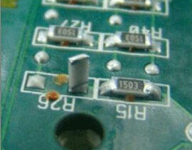
What is PCB Tombstoning and How to Prevent ItPCB tombstoning occurs when one end of a small SMT component, like a resistor or capacitor, lifts during soldering, causing it to stand upright. This defect results from uneven solder wetting forces.Key Causes:
- Uneven heating during reflow.
- Inconsistent solder paste application.
- Poor PCB design, such as asymmetrical pads.
- Component misalignment.Prevention Tips:
- Ensure uniform heating.
- Apply balanced solder paste.
- Follow proper PCB design practices.
- Align components accurately.By addressing these factors, manufacturers can minimize tombstoning and improve PCB reliability.
Blog
Understanding the Coefficient of Thermal Expansion (CTE) in PCBsIn the world of electronics, Printed Circuit Boards (PCBs) form the backbone of almost every device, from simple gadgets to complex systems. One critical aspect of PCB design that often goes unnoticed is the Coefficient of Thermal Expansion (CTE). Understanding CTE is vital for ensuring the reliability and longevity of electronic products.What is CTE?The Coefficient of Thermal Expansion (CTE) is a measure of how much a material expands or contracts when its temperature changes. For PCBs, CTE is typically expressed in parts per million per degree Celsius (ppm/°C). It indicates the rate at which the PCB material, such as the substrate or copper traces, will expand when heated and contract when cooled.Why is CTE Important in PCBs?In a PCB, different materials are combined—such as copper for traces and FR4 for the substrate. Each material has its own CTE, which means they expand and contract at different rates when subjected to temperature changes. If the CTE mismatch is significant, it can lead to mechanical stress within the PCB, causing warping, delamination, or even cracking. Over time, these stresses can compromise the electrical performance of the board, leading to failures.Managing CTE in PCB DesignDesigners must carefully consider the CTE values of all materials used in a PCB, especially in applications exposed to wide temperature ranges or frequent thermal cycling. For instance, FR4, a commonly used PCB substrate, has a CTE of around 10-16 ppm/°C below its glass transition temperature (Tg). However, once the temperature exceeds Tg, the CTE can increase dramatically, leading to potential reliability issues.To mitigate these risks, engineers can:- Select materials with matching CTEs: Using materials with similar CTEs can reduce stress between layers.
- Optimize layer stack-up: Proper layering and thickness can help distribute stress evenly across the board.
- Consider alternative materials: For high-reliability applications, materials with lower CTE values or higher Tg, such as ceramic substrates, might be used.ConclusionThe Coefficient of Thermal Expansion is a crucial factor in PCB design, directly impacting the board's reliability and performance. By understanding and managing CTE, engineers can ensure their designs withstand the thermal stresses of real-world operating conditions, leading to more durable and dependable electronic devices.
Blog
Understanding BGA Reballing: A Quick OverviewBGA (Ball Grid Array) reballing is a critical process in electronics repair and manufacturing. BGAs are chips with tiny solder balls on the underside that connect the chip to a circuit board. Over time, these solder balls can become damaged or require replacement if the chip needs to be reused or reinstalled.Reballing involves removing the old solder balls, thoroughly cleaning the chip, and applying new solder balls. This process restores the chip to its functional state, ensuring it can be properly reattached to a circuit board.While it may seem straightforward, BGA reballing is a precise process that requires specialized equipment and skilled technicians. It's an essential step in maintaining the reliability of electronic devices.
Blog
Press ReleaseSacramento PCB Assembly Achieves ISO 9001 and ISO 13485 CertificationsFOR IMMEDIATE RELEASEFolsom, CA – August 8, 2024 – Sacramento PCB Assembly, a leading provider of printed circuit board (PCB) assembly services, is proud to announce that it has been awarded ISO 9001:2015 and ISO 13485:2016 certifications. These prestigious certifications underscore our commitment to quality management and dedication to meeting the rigorous standards of the medical device industry.The ISO 9001:2015 certification is an internationally recognized standard that ensures the company's quality management system (QMS) consistently provides products and services that meet customer and regulatory requirements. This certification reflects Sacramento PCB Assembly's continuous improvement and customer satisfaction efforts.The ISO 13485:2016 certification specifically addresses the stringent requirements for a comprehensive QMS for the design and manufacture of medical devices. Achieving this certification demonstrates Sacramento PCB Assembly's ability to provide high-quality PCB assemblies that meet the exacting standards of the medical device industry."We are extremely proud to have achieved both ISO 9001 and ISO 13485 certifications," said Sam Miller , CEO of Sacramento PCB Assembly. "These certifications are a testament to our team's hard work, dedication, and commitment to excellence. They also reinforce our ability to deliver top-tier PCB assembly services to our clients, particularly in the medical device sector."Sacramento PCB Assembly has consistently focused on quality, innovation, and customer satisfaction. With these certifications, the company is well-positioned to expand its market presence and continue delivering reliable and high-quality PCB assemblies to its growing customer base.For more information about Sacramento PCB Assembly and its services, please visit www.sacramentopcbassembly.comMedia ContactRich Foreman
Marketing Consultant, Sacramento PCB Assembly
Email:rich.foreman@ansync.comAbout Sacramento PCB AssemblySacramento PCB Assembly is a premier provider of PCB assembly services, offering a wide range of solutions to various industries, including medical, aerospace, and consumer electronics. With a strong emphasis on quality, innovation, and customer satisfaction, the company is dedicated to delivering exceptional products and services that meet the highest industry standards.
Blog
What is a PCB Test Coupon?A PCB Test Coupon is a small section of a printed circuit board (PCB) that is used for quality control and testing purposes. These coupons are typically fabricated alongside the main PCB and are designed to mimic specific characteristics or features of the board. Here are the key aspects of PCB test coupons:Purpose and Function1. Quality Assurance:
- Electrical Testing: Test coupons help verify the electrical performance of the PCB, including impedance, continuity, and resistance.
- Structural Testing: They are used to check the integrity of the PCB layers, vias, and traces.
- Thermal Testing: Coupons may be used to test the thermal properties of the materials used in the PCB.2. Process Validation:
- Manufacturing Process Monitoring: Test coupons allow manufacturers to monitor the consistency and reliability of their production processes.
- Material Verification: They help ensure that the materials used meet the specified requirements and standards.3. Design Verification:
- Design Validation: Coupons can validate that the PCB design meets the necessary specifications and performance criteria.
- Prototyping: They are often used during prototyping to ensure that the design will function as intended when scaled up to full production.Types of Tests Conducted- Impedance Testing: To ensure signal integrity and compliance with design specifications.
- Microsection Analysis: Cross-sectioning the coupon to inspect the internal structure, layer alignment, and via quality.
- Solderability Testing: To check the surface finish and solderability of the PCB pads.
- Environmental Testing: To evaluate the PCB's performance under different environmental conditions, such as humidity and temperature.Design Considerations- Representative Layout: Test coupons are designed to include representative features of the main PCB, such as specific trace widths, via sizes, and material layers.
- Placement: They are typically placed on the edges of the PCB panel to avoid affecting the main PCB area.
- Standardization: Coupons may follow industry standards, such as IPC-2221 or IPC-6012, to ensure compatibility and consistency in testing.ImportancePCB test coupons are crucial for ensuring the reliability and performance of PCBs, especially in high-reliability applications like aerospace, medical devices, and telecommunications. They provide a cost-effective way to conduct thorough testing without damaging or altering the main PCB.
Blog
What is ENIG PCB Surface Finish?ENIG, or Electroless Nickel Immersion Gold, is a widely used surface finish in the Printed Circuit Board (PCB) industry. This process involves coating the copper traces of a PCB with a layer of nickel, followed by a thin layer of gold. The nickel layer acts as a barrier to prevent the diffusion of copper into the gold, while the gold layer provides a highly solderable surface and protects the nickel during storage.Key Advantages of ENIG1. Excellent Solderability: ENIG provides a flat, smooth surface that is ideal for soldering, making it compatible with fine-pitch components and ensuring reliable solder joints.2. Corrosion Resistance: The gold layer protects the nickel from oxidation, enhancing the PCB's durability and longevity.3. Wire Bonding Capability: ENIG is suitable for wire bonding applications, which is crucial in certain electronic assemblies.4. Planarity: The finish is extremely planar, making it well-suited for Surface Mount Technology (SMT) and ensuring proper component placement and performance.ApplicationsENIG is extensively used in various applications, including consumer electronics, telecommunications, automotive, aerospace, and medical devices. Its reliability and performance make it a preferred choice for high-end and mission-critical applications where precision and durability are paramount.Final ThoughtsENIG PCB surface finish combines excellent solderability, corrosion resistance, and planarity, making it a versatile and reliable choice for a wide range of electronic applications. Understanding its benefits can help manufacturers select the appropriate surface finish to ensure the optimal performance and longevity of their PCBs.
Blog
What is Hot Air Solder Leveling (HASL) PCB Surface Finish?Hot Air Solder Leveling (HASL) is a type of surface finish applied to printed circuit boards (PCBs) to prevent oxidation of the underlying copper, thereby ensuring solderability during the assembly process. The HASL process involves coating the PCB with molten solder and then using a hot air knife to level off the excess solder, leaving a thin layer of solder on the surface. This finish provides a reliable surface for soldering with good shelf life and is one of the oldest and most common types of PCB surface finishes.Benefits of HASL include:- Good Wetting Properties: HASL finishes provide excellent wetting properties, ensuring that solder properly adheres to the surface during the soldering process.
- Cost-Effectiveness: Compared to other surface finishes, HASL is generally more affordable.
- Long Shelf Life: The solder layer protects the copper traces from oxidation, contributing to a longer shelf life for the PCB.However, there are some drawbacks:- Uneven Surface: The leveling process can result in an uneven surface, which might not be suitable for fine-pitch components.
- Thermal Stress: The high temperatures used in the HASL process can cause thermal stress to the PCB, potentially affecting its reliability.
- Lead Concerns: Traditional HASL uses leaded solder, although lead-free alternatives are available, addressing environmental and health concerns associated with lead.In summary, HASL is a cost-effective and durable surface finish suitable for a wide range of applications, though it may not be the best choice for high-density or fine-pitch PCBs.
Blog
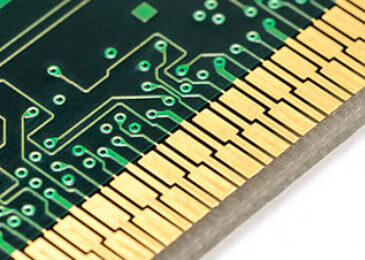
What are PCB Gold Fingers?
PCB Gold Fingers are critical components in the architecture of electronic devices, serving as the primary interface for connection between printed circuit boards (PCBs) and external systems or components. These gold-plated connectors are strategically positioned at the edge of PCBs, facilitating reliable and efficient communication, power transmission, and signal integrity across connected devices.The selection of gold for these connectors is attributed to its superior electrical conductivity and exceptional resistance to corrosion, qualities that ensure long-term reliability and performance in a wide range of environmental conditions. This makes PCB Gold Fingers indispensable in applications requiring high levels of precision and durability, from sophisticated computing hardware to high-performance gaming consoles.In essence, PCB Gold Fingers are a testament to the importance of material science and engineering in optimizing electronic device functionality. Their role in ensuring seamless interoperability and enhancing the longevity of electronic components underscores the meticulous design and engineering principles that underpin the modern digital ecosystem.
Blog
What are Fiducial Marks?
Fiducial marks are essential reference points on a Printed Circuit Board (PCB) used during the assembly process to ensure precise placement of components. These small, circular copper pads serve as alignment guides for assembly machines, helping to adjust for any slight warping or stretching of the PCB that may occur during manufacturing. They play a crucial role in maintaining the accuracy of component placement, thereby enhancing the overall quality and functionality of electronic devices.There are two main types of fiducial marks: global and local. Global fiducials provide a reference for the orientation and positioning of the entire PCB within the assembly machinery, similar to a map's cardinal directions. Local fiducials, conversely, focus on specific areas of the board, guiding the placement of components in those regions with greater precision. This system of global and local fiducial marks ensures that despite any physical irregularities in the PCB, the assembly process can be conducted with high accuracy, minimizing errors and potential device malfunctions.
Blog
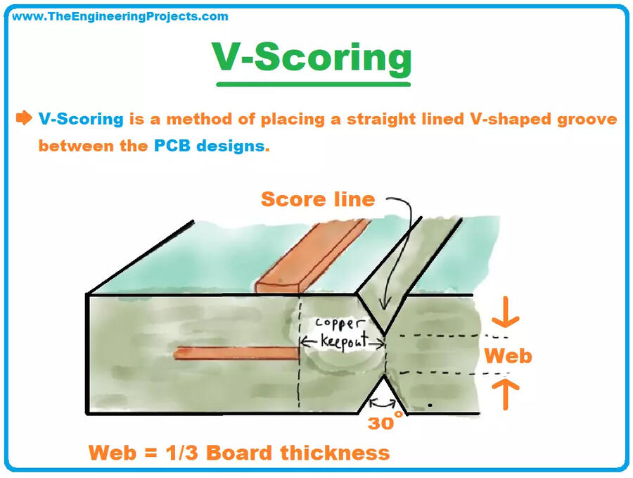
What is PCB V-Scoring?
PCB V-Scoring is a manufacturing process used in the production of printed circuit boards (PCBs) where a V-shaped groove is cut along both the top and bottom surfaces of the PCB panel. This groove is designed to facilitate the easy separation of individual boards from the panel after the assembly process is complete. The V-groove is typically cut to a predetermined depth, leaving a thin layer of material intact to hold the boards together during handling and assembly.This method allows multiple PCBs to be fabricated and assembled on a single panel, improving manufacturing efficiency and reducing costs. When the boards are ready to be separated, the V-Scoring allows them to be easily broken apart along the grooved lines, ensuring a clean and straight edge. V-Scoring is most suitable for straight-line separations and is commonly used for rectangular or square PCBs. For designs with irregular shapes or requiring more precise separations, other methods like tab-routing may be used instead.
Blog
What is a Polyester PCB Board?A Polyester PCB Board refers to a type of Printed Circuit Board (PCB) that uses polyester (PET or PEN) as the base material instead of the more common materials like FR4 (a fiberglass composite) or polyimide. Polyester materials are chosen for their flexibility, cost-effectiveness, and adequate thermal and electrical properties for certain applications.The key features of Polyester PCBs include:1. Flexibility: Polyester materials are inherently more flexible than traditional rigid PCB materials. This makes Polyester PCBs suitable for applications where the board may need to bend or flex during its use, such as in flexible electronics, wearable devices, and some types of sensors.2. Cost-Effectiveness: Compared to high-end materials like polyimide, polyester is generally less expensive. This makes it an attractive option for applications where cost is a critical factor.3. Thermal and Electrical Properties: While not as high-performing as some other materials under extreme conditions, polyester still offers adequate thermal resistance and electrical insulation for many low to medium performance applications.4. Environmental Resistance: Polyester PCBs have good resistance to chemicals, solvents, and moisture, which makes them suitable for use in harsh environmental conditions.Polyester PCBs are most commonly used in the manufacture of flexible circuits, but their specific properties limit their use to applications where high temperatures and high performance are not critical. They are a good choice for disposable electronics, flexible displays, and other innovative electronics where flexibility and cost are more important than the highest levels of performance.
Blog
What is a Copper Weight?
Copper weight in a Printed Circuit Board (PCB) refers to the thickness of the copper layer that is used on the board. It is an important parameter in PCB design and manufacturing, as it affects the electrical properties and thermal performance of the board. Copper weight is usually measured in ounces per square foot (oz/ft²) and indicates how much copper is present on one square foot of the board area.The most common copper weights used in PCBs are:**1 oz/ft²: **This is the standard copper thickness used for many applications, providing a good balance between cost, conductivity, and heat dissipation.
**2 oz/ft²: **Thicker copper used for higher power applications, where increased current carrying capacity and thermal management are necessary.
**0.5 oz/ft²: **Thinner copper used for fine line applications, such as high-density interconnect (HDI) PCBs, where space is at a premium.Heavier copper weights increase the PCB's ability to conduct electricity and dissipate heat but also make the board thicker and more expensive. The choice of copper weight depends on the specific requirements of the electronic device, including its power levels, thermal management needs, and the precision of the electronic signals it carries.
Blog

What are Halogen Free PCB Boards?
Halogen-free PCB (Printed Circuit Board) boards are types of PCBs that are manufactured without the use of halogenated compounds, specifically materials that contain chlorine (Cl) or bromine (Br) as part of their composition. These elements are commonly found in flame retardants, which are added to traditional PCB materials to reduce the risk of fire. However, halogens can release toxic and corrosive gasses when burned or heated to high temperatures, posing environmental and health risks.The push towards halogen-free PCBs is part of a broader effort to create more environmentally friendly and safer electronic components. By avoiding halogenated flame retardants, halogen-free PCBs aim to:1. Reduce Toxic Emissions: During manufacturing, recycling, or in the event of a fire, halogen-free PCBs release fewer toxic and corrosive gasses.
2. Improve Recyclability: The absence of halogens makes the recycling process of PCBs less hazardous and more efficient.
3. Enhance Safety: Reducing the use of halogens lowers the risk of exposure to toxic substances for both workers in manufacturing facilities and end-users.Halogen-free PCBs often use alternative materials for flame retardancy, such as phosphorus-based compounds, which have a lesser impact on the environment and human health. These boards are particularly important in applications where safety, environmental impact, and sustainability are key concerns, such as in consumer electronics, automotive, and medical devices.The transition to halogen-free PCBs involves challenges, including the need to ensure that the alternative materials meet the performance standards required for different applications, such as thermal stability, electrical performance, and mechanical strength. Manufacturers must also consider the cost implications, as halogen-free materials can be more expensive than traditional ones.Overall, halogen-free PCBs represent an important step towards reducing the environmental footprint of electronic devices and improving safety standards in the electronics industry.
Blog
Best Practices for PCB DesignDesigning a Printed Circuit Board (PCB) is a complex task that requires a careful balance of electrical performance, reliability, manufacturability, and cost. As electronic devices continue to evolve, becoming more compact and integrated, the importance of efficient and effective PCB design has never been greater. We will outline best practices in PCB design, drawn from industry standards and experienced professionals' insights, to ensure the success of your electronic projects.1. Understand Your Requirements
Before starting the design process, clearly understand the requirements of your PCB. This includes the purpose of the board, the environment it will operate in, the expected lifespan, and any size or shape constraints. These factors will influence many of your design decisions.2. Plan for EMI/EMC Compliance
Electromagnetic interference (EMI) and electromagnetic compatibility (EMC) are critical considerations for PCB design. To minimize EMI and ensure EMC compliance, use proper grounding techniques, place decoupling capacitors close to power pins of ICs, and consider the routing of high-speed signals carefully to avoid interference.3. Optimize Component Placement
The placement of components on a PCB dictates not only the board's functionality but also its manufacturability and performance. Place components in a way that minimizes the length of critical signals, reduces the possibility of EMI, and facilitates easier soldering and testing. Group related components together and consider thermal management and mechanical constraints.4. Adopt a Robust Power Distribution Network (PDN)
A well-designed PDN is essential for the stable operation of the board. Ensure that power and ground layers are adequately planned to minimize voltage drops and impedance. Use thick traces or planes for power and ground paths to handle the current requirements efficiently.5. Signal Integrity and Routing
Signal integrity is crucial for the reliable performance of high-speed circuits. Maintain consistent impedance across traces, use differential pairs for high-speed signals, and avoid sharp turns which can cause signal reflections. Also, consider the use of vias carefully, as they can impact signal integrity and add parasitic capacitance and inductance.6. Thermal Management
Effective thermal management is essential to prevent overheating, which can affect performance and reliability. Use thermal vias to transfer heat away from power components, consider the placement of heat sinks, and ensure that there is adequate airflow around components that generate heat.7. Design for Manufacturability (DFM)
Design your PCB with manufacturability in mind to avoid costly revisions and production delays. This includes using standard component footprints, avoiding fine-pitch components when possible, and ensuring that there is sufficient spacing between components for assembly. Consult with your manufacturer early in the design process to understand their capabilities and limitations.8. Test and Validation
Design your board with testing in mind, including test points for critical signals and power rails. Use simulation tools to validate your design before prototyping, and once prototypes are built, perform thorough testing under conditions that mimic real-world use.9. Documentation and Review
Comprehensive documentation is vital for troubleshooting, future revisions, and compliance with regulatory standards. Include a detailed bill of materials (BOM), assembly drawings, and schematics. Before finalizing your design, conduct a thorough review with your team, and consider having it reviewed by an external expert if possible.10. Continuous Learning and Adaptation
PCB design is an ever-evolving field with new technologies, materials, and methodologies being developed regularly. Stay informed about industry trends, new tools, and best practices through continuous learning and adaptation.By following these best practices, you can ensure that your PCB design is robust, reliable, and ready for the challenges of modern electronics. Remember, a successful PCB design is the result of careful planning, attention to detail, and collaboration with your team and manufacturing partners.
Blog

What is Solder Mask?
A solder mask, often referred to as solder resist, is a thin protective layer of polymer that is applied to the copper traces of a Printed Circuit Board (PCB). This layer serves multiple purposes, the most significant being to prevent accidental solder bridging between conductive tracks, pads, or vias, which could lead to short circuits. It also protects the copper from environmental damage, such as oxidation, which can degrade the board over time.
Purpose of Solder Mask
The primary purposes of the solder mask in PCB design and manufacturing include:
Preventing Short Circuits: By covering the non-solderable surfaces, the solder mask ensures that solder does not connect two points on the board that should not be connected.
Protection Against Oxidation: Exposed copper can oxidize when exposed to air, leading to poor solderability and potential circuit failure. The solder mask layer helps protect these copper traces.
Reducing Corrosion: By sealing off the copper traces, the solder mask helps prevent corrosion caused by exposure to moisture and other corrosive elements.
Enhancing Aesthetics: Solder masks give PCBs their characteristic appearance and can be applied in various colors, with green being the most common due to its ease on the eyes during inspection and its ability to show contrast with traces and pads.
Types of Solder Mask
There are several types of solder masks available, each with its application method and specific use cases. These include:
Liquid Photo-Imaginable (LPI) Solder Mask: This is the most common type used in PCB production. It is applied in liquid form and then cured with UV light. LPI solder masks are known for their fine resolution and suitability for complex PCB designs.
Dry Film Solder Mask: This type comes in a pre-dried film that is applied using heat and pressure. It is typically used for high-volume production.
Top and Bottom Solder Mask: This refers to the application of solder mask material to both the top and bottom layers of a PCB to provide double-sided protection.
Importance of Solder Mask in PCB Design
The inclusion of a solder mask in PCB design is critical for several reasons:
Improving PCB Lifespan: By preventing oxidation and corrosion, the solder mask significantly extends the life of a PCB.
Enhancing Performance: By preventing short circuits, the solder mask ensures that the PCB performs as designed, without unexpected failures.
Facilitating High-Density Design: With the advancement of technology, PCBs are becoming more compact. The solder mask helps in creating and maintaining the integrity of fine lines and spacing, essential for high-density interconnect (HDI) boards.
The solder mask is a vital component of PCBs, offering protection against physical and chemical damage, preventing short circuits, and enhancing the overall durability and functionality of the board. As PCB designs become more complex and miniaturized, the role of the solder mask in ensuring the reliability and performance of electronic devices becomes even more critical.
Blog
PCB Silkscreen Layer Explained
The silkscreen on a Printed Circuit Board (PCB) is not just a layer of aesthetics; it plays a critical role in the board's functionality and assembly. Acting as the visual guide on a PCB, the silkscreen layer features text and symbols printed directly on the surface, detailing component labels, instructions, and other vital information in high-contrast ink—usually in stark white or bold black.Purpose and Functionality
Silkscreen does more than identify components; it provides essential assembly instructions, enhances the PCB's appearance, and aids in quality control. This layer facilitates accurate and efficient assembly, troubleshooting, and maintenance by clearly marking component positions, orientations, and other guidelines. Its resilience against manufacturing processes ensures longevity and readability.Creation and Application
The process of incorporating a silkscreen layer involves several precise steps:Design: Utilizing CAD software, designers create the silkscreen layer, embedding all necessary markings.Screen Printing: The design is transferred onto the PCB through screen printing, where ink is applied over a stencil, mapping out the required text and symbols.Curing: The applied ink is cured, typically via heat or UV light, to secure its adherence and durability.Inspection: The final step is a thorough inspection to ensure the accuracy and clarity of the silkscreen, crucial for the PCB's usability and assembly efficiency.This meticulous application process ensures the silkscreen serves its purpose effectively, guiding assembly processes, and enhancing the PCB's functionality and reliability.Impact and Importance
The silkscreen layer, though seemingly minor, is indispensable in PCB design. It simplifies the assembly process, aids in the identification and troubleshooting of components, and ensures the product's quality and performance. The precision in creating and applying the silkscreen underscores its significance in the lifecycle of electronic devices, proving that it is much more than a mere label or decoration on a PCB.
Blog
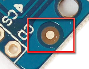
What is an Annular Ring?An annular ring is the copper ring surrounding a plated through-hole on a PCB, forming the connection point for component leads or vias. Its width is the distance between the hole's edge and the copper pad’s edge.Importance of the Annular Ring1. Electrical Connection: It ensures a stable electrical connection and a reliable solder joint.
2. Mechanical Strength: Adds strength to the hole, protecting against damage.
3. Manufacturing Tolerances: Compensates for drilling misalignments.
4. Thermal Management: Larger rings can help in heat dissipation.Design Considerations- Size: Balance between too small (risking breakage) and too large (wasting space).
- Manufacturing Capabilities: Smaller rings require more precise, costly manufacturing.
- Application Needs: High-reliability sectors might need larger annular rings.
- Thermal Stress: Allow for expansion in high-temperature environments.Common Challenges- Drilling Accuracy: Misaligned holes can reduce the ring’s effectiveness.
- Pad Size vs. Ring Size: In dense designs, pad size reduction can compromise the ring.
- Cost vs. Reliability: Precision manufacturing costs versus the need for reliable rings.ConclusionThe annular ring, a small but pivotal part of the PCB, significantly influences the board's functionality and reliability. Proper understanding and design considerations are vital for efficient, durable PCBs.
Blog
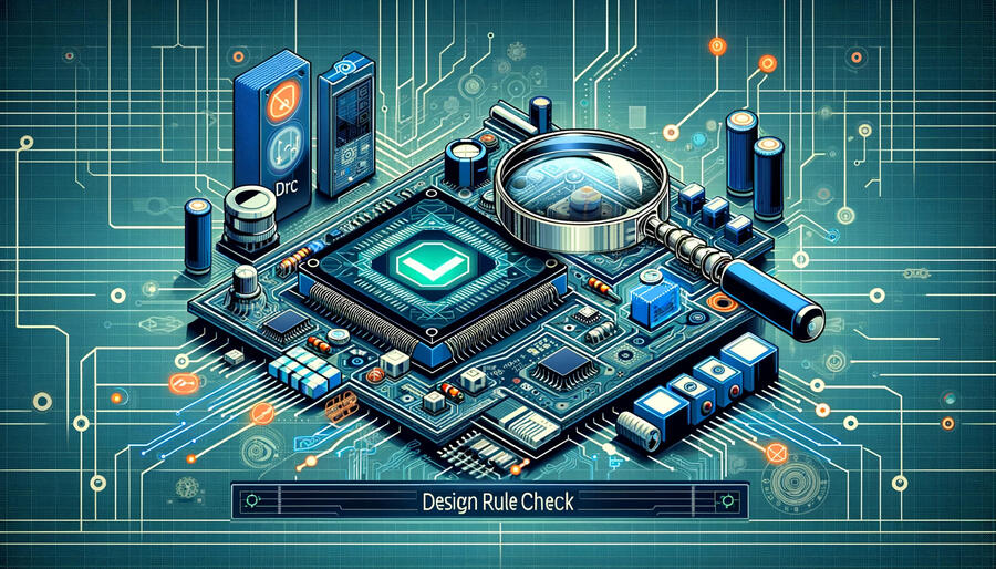
Understanding Design Rule Check (DRC) in PCB ManufacturingDesign Rule Check (DRC) plays a pivotal role in PCB manufacturing. DRC is an automated process in PCB design software, crucial for ensuring the manufacturability and functionality of printed circuit boards.Key Aspects of DRC- What is DRC? It's a process that checks a PCB design against specific rules to identify and rectify potential manufacturing and functionality issues.- Importance of DRC: It prevents manufacturing errors, ensures reliability and compliance with industry standards.- How DRC Works: The process involves validating aspects like trace widths, hole sizes, and component spacing against predefined rules. Violations are flagged for correction.Tips for Effective DRC Usage1. Know Manufacturer Specifications: Tailor DRC rules to the capabilities and limitations of your chosen PCB manufacturer.2. Run Regular Checks: Frequently check your design with DRC to catch and rectify errors early.3. Update Rules Regularly: Adjust your DRC rules to keep pace with evolving technology and standards.ConclusionDRC is an essential tool in PCB design, acting as a gatekeeper to ensure designs are ready for manufacturing. By effectively leveraging DRC, designers can enhance the quality of their PCBs, ensuring they are both functional and reliable. In the world of PCB design, DRC is an indispensable ally for achieving excellence.
Blog
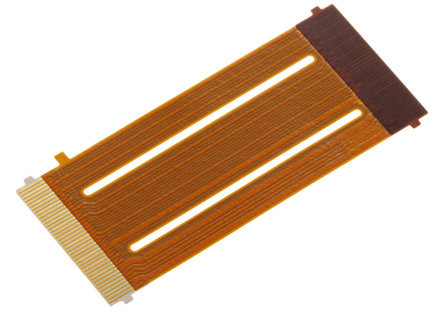
High-Heat-Resistant Flexible Printed Circuit Board YFLEXYamaichi Electronics has introduced a heat-resistant version of their YFLEX flexible printed circuit board (FPC), designed for high-temperature environments up to 150°C. This FPC maintains its electrical properties for over 3,000 hours, with a continuity resistance change of ±10% and insulation resistance above 500 MΩ. Ideal for automotive, semiconductor manufacturing, and test and measurement applications, the YFLEX features an improved insulating layer with enhanced adhesion due to a special cover layer.The PCB, versatile in design, is available in single or double-layer configurations, with liquid crystal polymer (LCP) or polyimide (PI) as insulation substrate options. It also includes a reinforced GND design, making it suitable for environments requiring high heat and noise resistance.
Blog
Exploring Blind Vias in PCB Design
Overview:Blind vias are essential in modern multi-layer Printed Circuit Boards (PCBs). They connect an outer layer to one or more inner layers, optimizing space and enhancing performance in compact electronics.Function and Advantages:Space Efficiency: Ideal for high-density designs, blind vias allow for more components within limited spaces.
Enhanced Performance: They shorten signal paths and reduce interference, crucial for high-speed circuits.
Design Flexibility: These vias provide more options in routing layers, essential for complex PCBs.Creation Methods:Blind vias are made using either mechanical drilling, which is precise but costly, or laser drilling, suitable for creating smaller, high-density vias.Applications:Widely used in smartphones, wearable devices, computer motherboards, and aerospace technology, blind vias meet the demands for compactness and functionality.Challenges:Manufacturing blind vias involves complex, expensive processes and can lead to reliability issues if not properly implemented. Designers must navigate these challenges with precise planning.Conclusion:Blind vias are key in evolving PCB design, offering space efficiency and performance enhancement. Their growing importance parallels the advancement in electronic device technology.
Blog
What is a Buried Via?
Introduction:In the intricate world of printed circuit board (PCB) design, understanding the myriad of components and techniques is crucial for creating efficient and effective electronic devices. One such component, often overlooked but vital, is the 'buried via'. Let's delve into what a buried via is, its applications, and why it's essential in modern PCB design.Defining a Buried Via:A 'via' in PCB terminology refers to a pathway that connects different layers of a PCB. Vias are essentially conductive holes filled with or plated with metal that allow electrical connection between layers. Among the various types of vias, the 'buried via' has a unique characteristic: it connects internal layers of the PCB but is not visible from the surface.Key Characteristics:Invisibility from the Surface: Unlike through-hole vias that go through the entire board, or blind vias that connect an outer layer to an inner one, buried vias are completely hidden within the internal layers.Complex Manufacturing: The creation of buried vias involves advanced PCB manufacturing techniques. Layers containing these vias are first created and then laminated together with the rest of the PCB layers.Space Efficiency: By not penetrating the entire board, buried vias free up space on the external layers, which is crucial for high-density designs.Applications in PCB Design:High-Density Boards: In compact electronics like smartphones, space is a premium. Buried vias allow for more components on the surface layers by utilizing the inner layers for connections.Improved Signal Integrity: By allowing shorter paths and reducing interference, buried vias can enhance the performance of high-speed circuits.Enhanced Aesthetics and Protection: For devices where the appearance of the PCB is important, or where surface protection is needed, buried vias keep the surface neat and unobstructed.Challenges and Considerations:Cost and Complexity: The manufacturing process for buried vias is more complex and costly than standard vias. This needs to be weighed against the benefits in high-density and high-performance applications.Design Constraints: Using buried vias requires careful planning in the PCB design phase to ensure that all connections are correctly made and accessible for testing.Thermal Management: As these vias are buried, they can sometimes pose challenges in heat dissipation, requiring careful thermal management planning.Conclusion:Buried vias, while not visible on the surface, play a critical role in modern PCB design. They offer solutions for space efficiency, signal integrity, and aesthetics, especially in compact and high-performance electronic devices. However, their benefits come with considerations of cost, complexity, and design constraints. Understanding the role of buried vias is essential for anyone involved in PCB design and manufacturing, as it opens up possibilities for more innovative and efficient electronic designs.
Blog
Decoding Vias in PCB Design
Overview
Vias are a critical element in Printed Circuit Board (PCB) design, serving as conduits for electrical signals between different layers of the board. This concise guide explores the types, functions, and significance of vias in PCBs.
What is a Via?
A via is a small hole in a PCB that allows electrical connections across different layers, akin to a tunnel for electrical signals.
Types of Vias
Through-Hole Vias: Connect all layers from top to bottom.
Blind Vias: Link an outer layer to internal layers, not visible from the PCB surface.
Buried Vias: Connect only internal layers, invisible from the outside.
Functions
Electrical Connection: Vias primarily create paths for electrical signals across PCB layers.
Heat Dissipation: They assist in managing heat in high-power circuits.
Signal Integrity: Strategic via placement can enhance signal clarity and reduce path length.
Significance in PCB Design
pace Efficiency: Vias enable compact designs by facilitating layer-to-layer connections.
Design Flexibility: They allow for more complex circuitry, especially in multi-layer PCBs.
Performance Boost: Properly used vias can improve PCB performance by optimizing signal routes.
Challenges
Cost: Advanced vias like blind and buried types can increase PCB production costs.
Complexity: More vias can complicate design and manufacturing.
Reliability Risks: Inadequately designed vias can lead to signal loss or damage.
Conclusion
Vias are indispensable in PCB design, allowing for more complex, high-performance, and space-efficient electronic devices. Understanding their types, functions, and design implications is key to effective PCB creation.
Blog
The Advantages of High Tg PCB in Electronics DesignUnderstanding High Tg PCBIn the world of electronics, the term 'PCB' is quite familiar. PCB stands for Printed Circuit Board, a fundamental component in electronic devices. However, not all PCBs are created equal. Among the various types, High Tg PCBs have gained significant attention for their enhanced performance in demanding environments.What is High Tg PCB?Tg stands for Glass Transition Temperature. It's the temperature point at which the PCB material begins to transform from a hard, glassy state to a soft, pliable state. A High Tg PCB has a higher glass transition temperature compared to standard PCBs. This higher Tg value means the PCB can withstand more heat before it begins to deform.Why Choose High Tg PCB?Enhanced Thermal StabilityThe primary advantage of High Tg PCB is its superior thermal stability. Devices are getting smaller, and circuits are getting more complex, leading to higher heat generation. High Tg PCBs can withstand higher temperatures, making them ideal for high-density and high-power applications.Improved Durability and ReliabilityThese PCBs are less likely to break down or malfunction under high-temperature conditions, ensuring a longer lifespan for the device. This reliability is crucial in industries like aerospace, automotive, and military applications, where failure is not an option.Better Chemical and Moisture ResistanceHigh Tg PCBs offer enhanced resistance to chemicals and moisture. This quality is essential in harsh environments, such as outdoor telecommunications equipment or industrial machinery exposed to chemicals.Reduced Thermal ExpansionAs temperatures rise, materials expand. High Tg PCBs have a lower rate of thermal expansion, which means less stress on the solder joints and components. This property is particularly important in lead-free soldering processes, which require higher temperatures.Applications of High Tg PCB1. Automotive Industry: With the rise of electric vehicles and advanced driver-assistance systems, the demand for reliable and heat-resistant PCBs is paramount.2. Aerospace and Defense: These sectors require components that can withstand extreme conditions, making High Tg PCBs an ideal choice.3. Consumer Electronics: As devices become smaller and more powerful, managing heat becomes a critical challenge that High Tg PCBs can address.4. Industrial Applications: In environments with high temperatures or exposure to chemicals, High Tg PCBs provide the necessary durability.5. LED Lighting: LEDs generate a significant amount of heat, making High Tg PCBs a suitable option for LED lighting systems.ConclusionIn summary, High Tg PCBs are a remarkable innovation in the field of electronics. They offer enhanced thermal stability, reliability, and durability, making them ideal for applications where standard PCBs might fail. As technology continues to evolve and the demand for more powerful and compact devices grows, High Tg PCBs will undoubtedly play a critical role in the future of electronics design.
Blog

The Elemental Composition of Recycled PCB PowderA recent study by Shintaro Ichikawa and colleagues at Fukuoka University focused on analyzing the elemental composition and durability properties of powdered printed-circuit boards (PCBs). They utilized a process called cryo-milling to produce the powder and then applied X-ray fluorescence (XRF) and X-ray diffraction (XRD) for detailed analysis. This research revealed varying concentrations of elements like aluminum, silicon, and copper in different particle fractions, each displaying unique elemental concentrations and durability characteristics. This investigation is significant in enhancing our understanding of electronic waste recycling, contributing to the development of more sustainable recycling practices.For more information, see the full article in the Spectroscopy
Blog

The U.S.'s Journey to Rebuild its Printed Circuit Board IndustryThe United States is currently making efforts to rejuvenate its printed circuit board (PCB) industry, which holds significant importance for national security and technological leadership. The U.S.'s global PCB production share has diminished, contrasting with China's growing dominance. This initiative involves government funding and new legislative measures aimed at enhancing domestic PCB production capabilities. The undertaking faces challenges such as competing with well-subsidized international producers and advancing manufacturing technologies. PCBs are vital for various sectors, including defense, computing, and infrastructure.For more information, see the full article in the EE Times
Blog
What is an HDI PCB Board?HDI PCBs are a type of circuit board with a higher wiring density per unit area compared to traditional PCBs. The "High-Density Interconnector" term signifies the dense connections of components on the board. These boards utilize finer lines and spaces, smaller vias (holes), and capture pads, enabling more compact, efficient designs.Key Features:1. Miniaturized Components: HDI PCBs allow for smaller components, reducing the size and weight of the final product.
2. Increased Circuit Density: The design accommodates more components per unit area, enhancing functionality.
3. Improved Electrical Performance: The compact design leads to shorter signal paths, reducing signal loss and cross-talk.
4. Enhanced Reliability: Tighter build standards increase the reliability of these boards in demanding conditions.How HDI PCBs Are MadeThe manufacturing process of HDI PCBs involves several advanced techniques:- Microvia Technology: Utilizes laser drilling to create small vias, enabling layer-to-layer connections with less space.
- Sequential Lamination: Multiple lamination cycles are used to build up the PCB layers, allowing for a more complex and dense design.
- Fine Line Technology: Enables narrower lines and spaces, increasing the wiring density.Applications of HDI PCBsHDI technology is crucial in various fields:- Consumer Electronics: Smartphones, laptops, and wearables heavily rely on HDI PCBs for their compact designs.
- Medical Devices: Essential in small, high-performance devices like pacemakers and hearing aids.
- Automotive Industry: Used in advanced driver-assistance systems (ADAS) and other compact electronic systems.
- Aerospace and Defense: Vital for high-density, reliable circuitry in space-constrained environments.Benefits of Using HDI PCBs1. Space Efficiency: Enables more compact and lightweight designs.
2. Enhanced Performance: Improves signal integrity and reduces noise.
3. Higher Component Density: Supports more functionality in a smaller area.
4. Design Flexibility: Allows for innovative designs due to the ability to incorporate different technologies.Challenges and ConsiderationsWhile HDI PCBs offer numerous advantages, they also pose some challenges:- Manufacturing Complexity: Requires advanced manufacturing capabilities and higher precision.
- Cost: Generally more expensive than traditional PCBs due to the complex manufacturing process.
- Design Expertise: Requires a higher level of design expertise to fully utilize the potential of HDI technology.ConclusionHDI PCBs represent a significant leap in PCB technology, driving innovation in numerous industries. Their ability to pack more functionality into a smaller space, combined with improved electrical performance and reliability, makes them indispensable in the era of miniaturization and high-performance electronics. As technology continues to evolve, HDI PCBs will undoubtedly play a pivotal role in shaping future electronic designs. Whether you're a seasoned engineer or a tech enthusiast, understanding HDI PCBs is key to grasping the future of electronic product development.
Blog
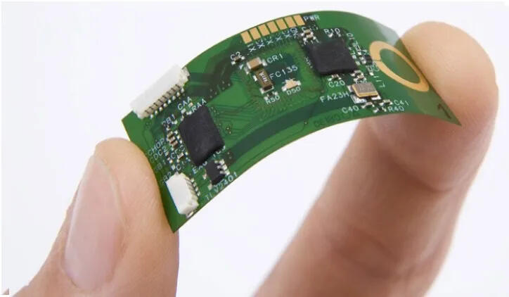
Flexible Printed Circuit Boards (FPCBs) ExplainedOverviewFlexible Printed Circuit Boards (FPCBs) are a modern innovation in electronics, distinguished by their ability to flex and bend. Made from materials like polyimide, they connect and support electronic components, offering a dynamic alternative to traditional rigid PCBs.ManufacturingFPCBs undergo a precise process, starting with a digitally designed layout. The chosen material, often polyimide, is then imprinted with conductive pathways using techniques like photolithography. After mounting electronic components, typically through surface-mount technology, these boards are rigorously tested for reliability.BenefitsFPCBs stand out for their:1. Flexibility: Ideal for tight or complex spaces.
2. Lightweight Design: Significantly thinner and lighter than traditional PCBs.
3. High Reliability: Capable of withstanding stress and vibration.
4. Efficient Heat Dissipation: Better heat management, ensuring component longevity.ApplicationsThese boards are not limited to consumer electronics. They're integral in sectors like medical devices, automotive, aerospace, and wearable technology, offering compact and flexible solutions.ConclusionFPCBs mark a significant shift in electronic design, accommodating the trend towards miniaturization and versatility. As technology evolves, their role in enabling smaller, more efficient devices will only grow, making them a cornerstone in future electronic advancements.
Blog

Strengthening National Defense: U.S. Invests $39.9 Million in Domestic Circuit Board ProductionThe U.S. Department of Defense is significantly strengthening America's supply chain security by granting Calumet Electronics Corporation a $39.9 million contract through the Defense Production Act Investment Program. Aimed at boosting High-Density Build-Up substrate production — crucial for advanced Printed Circuit Boards — this investment aligns with the Biden Administration's strategy to develop domestic capabilities in this critical sector, as underscored by Assistant Secretary of Defense Dr. Laura Taylor-Kale. Calumet, a Michigan-based firm, will use the funds to enhance its production of these vital components, pivotal for modern radar, electronic warfare, and communication systems. This grant is a key part of the DPAI Program's 2023 agenda, which includes 22 awards totaling $714 million, managed under the Manufacturing Capability Expansion and Investment Program, showcasing a strategic commitment to augmenting U.S. defense and technology sectors internally.Source: https://www.defense.gov/News/Releases/Release/Article/3589418/dod-awards-399-million-to-strengthen-us-supply-chains-for-printed-circuit-boards/
Blog
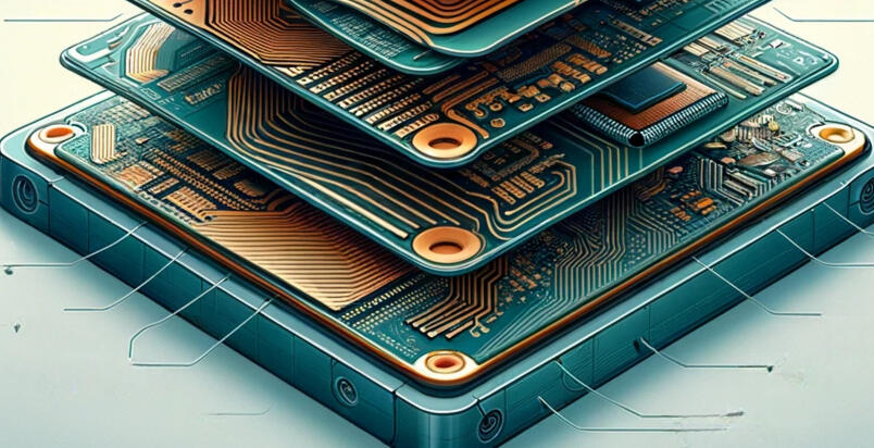
An Overview of Rigid-Flex PCBsIntroduction
In the world of electronics, innovation is key, and Rigid-Flex Printed Circuit Boards (PCBs) stand as a prime example of technological advancement. Merging the best of both rigid and flexible PCBs, Rigid-Flex PCBs have revolutionized the way electronic devices are designed and manufactured.What is a Rigid-Flex PCB?
A Rigid-Flex PCB is a hybrid circuit board that combines elements of rigid and flexible circuitry. This type of PCB includes rigid substrates that are joined with flexible interconnections. The result is a board that can be designed to fit into tight or unusual spaces, allowing for more creative and compact device designs.The Composition
Rigid-Flex PCBs are composed of multiple layers of flexible circuit substrates attached to rigid boards. The flexible layers are typically made from materials like polyimide or similar polymers, which provide excellent electrical properties and can withstand extreme temperatures. The rigid sections are usually made from fiberglass-reinforced epoxy resin.Advantages
1. Space and Weight Reduction: One of the key benefits of Rigid-Flex PCBs is the significant space and weight savings they offer. Their ability to bend and fold allows them to occupy less space, making them ideal for compact electronic devices like smartphones and wearable technology.2. Improved Reliability: By reducing the need for connectors and cables between rigid parts, these PCBs enhance reliability. Fewer connectors mean fewer potential points of failure, leading to more robust and dependable electronic systems.3. Enhanced Design Capabilities: Rigid-Flex PCBs offer unparalleled design flexibility. They can be tailored to fit unique shapes, which is especially beneficial in sophisticated electronics where space is at a premium.4. Reduced Assembly Time and Cost: Integrating both rigid and flex circuits into a single board simplifies the assembly process. This integration can lead to reduced assembly time and cost, as fewer parts need to be handled and installed.Applications
Rigid-Flex PCBs are used in various applications, from consumer electronics to aerospace and medical devices. Their versatility makes them suitable for complex, high-density circuit designs, especially where reliability and space-saving are crucial.Challenges
While Rigid-Flex PCBs offer many benefits, they also come with challenges. Designing these boards requires specialized skills and software. Moreover, the manufacturing process is more complex compared to traditional PCBs, often resulting in higher costs.Conclusion
Rigid-Flex PCBs are a pivotal innovation in the field of electronic design and manufacturing. By offering unparalleled flexibility, reliability, and space-saving features, they enable the creation of more compact, efficient, and robust electronic devices. As technology continues to advance, the role of Rigid-Flex PCBs is likely to become even more significant, paving the way for further innovation in electronic design.
Blog
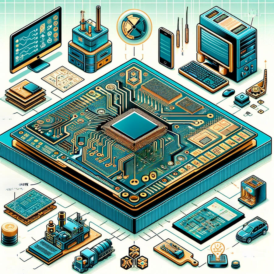
An Overview of Rigid PCBsIntroduction
Printed Circuit Boards (PCBs) are the backbone of modern electronics, and among them, Rigid PCBs hold a pivotal role. This article delves into the world of Rigid PCBs, explaining their nature, applications, and advantages, helping you understand why they are essential in today's technology.What is a Rigid PCB?
A Rigid PCB is a type of PCB that, as the name suggests, is inflexible. It's constructed from solid, rigid substrate materials like fiberglass, which prevent the board from twisting. Unlike their flexible counterparts, Rigid PCBs are sturdy and maintain their shape under normal conditions.Composition and Manufacturing
The process of creating a Rigid PCB involves several key components and manufacturing steps. Here's a look at its typical composition:
1. Substrate Layer: The base, usually made of fiberglass, provides strength and rigidity.
2. Copper Layer: This conductive layer has etched copper tracks creating circuit pathways.
3. Solder Mask: Applied over the copper layer, this insulates and protects against short circuits.
4. Silkscreen Layer: Used for labeling and adding symbols for easier assembly and troubleshooting.In manufacturing, a Rigid PCB goes through stages like material selection, pattern etching, drilling, plating, and testing to ensure it meets specific standards and requirements.Applications
Rigid PCBs are integral to a multitude of electronic devices. Their applications span various sectors:
- In Consumer Electronics: They are found in smartphones, computers, TVs, and home appliances.
- Within Industrial Equipment: They are used in machinery control systems and power equipment.
- In Medical Devices: Rigid PCBs are essential for diagnostic and monitoring equipment.
- For the Automotive Sector: They play a role in control systems and infotainment units.Advantages
Choosing a Rigid PCB comes with several benefits:
1. Durability: Their rigidity makes them durable and resistant to physical stress.
2. Ease of Assembly: The rigidity simplifies the soldering process of components.
3. High-Density Applications: They can accommodate more components in a smaller area.
4. Reliability: They are less prone to breakage and bending, enhancing longevity and performance.Considerations for Choosing a Rigid PCB
When selecting a Rigid PCB, several factors should be considered:
- Size and Layout: It's important to ensure that the PCB fits the intended space and supports the required circuit complexity.
- Material Quality: Opting for higher quality materials can improve performance and durability.
- Manufacturing Tolerances: Tighter tolerances mean better precision but come with a higher cost.
- Cost: The budget can influence the choice of materials and the complexity of the design.Conclusion
Rigid PCBs are a fundamental component in the realm of electronics. Their reliability, durability, and ease of use make them the preferred choice for a wide range of applications. Understanding their composition, manufacturing process, and applications can help in making informed decisions for any electronic design or project.
Blog

PCB Material Selection: Strategizing a Cost-Effective MixIn the intricate world of electronics manufacturing, the selection of Printed Circuit Boards (PCBs) materials stands as a critical decision point that can significantly impact both performance and cost. For entrepreneurs and engineers alike, the challenge is to strike a delicate balance between quality and expense. This is where the art of mixing PCB materials emerges as a strategic approach to gain a cost advantage without compromising on the essential performance characteristics.Understanding the BasicsBefore diving into the strategy of material mixing, it's essential to understand the core materials used in PCB manufacturing. The base material, often referred to as the substrate, is typically made of fiberglass (FR4 being the most common), Teflon, or a blend of other composites. The choice of substrate influences the PCB's thermal resistance, durability, and electrical properties.The Cost-Performance SpectrumHigh-performance materials like Teflon offer exceptional electrical characteristics, which are crucial for high-frequency applications. However, they come with a higher price tag. On the other end, standard materials like FR4 are cost-effective but may not meet the demands of advanced electronic applications.Mixing Materials: A Cost-Effective StrategyThe concept of mixing PCB materials involves using different materials in different layers or sections of the PCB to optimize both cost and performance. Here's how you can approach this strategy:1. Identify Performance RequirementsBegin by delineating the performance requirements of your PCB. High-speed signals, thermal management, and mechanical strength are some of the factors to consider. This step is crucial as it will guide you on where you can afford to use less expensive materials and where high-performance materials are non-negotiable.2. Segment Your PCB DesignDivide your PCB into segments based on functionality. High-frequency circuits may require materials with a low dielectric constant, while power circuits might need materials with higher thermal conductivity. By segmenting the design, you can apply high-performance materials selectively.3. Choose Your Material MixFor the segments that demand high performance, opt for materials like Rogers or Teflon. For less critical sections, standard FR4 can suffice. This selective placement can lead to substantial cost savings while maintaining the desired performance.4. Consult with SuppliersEngage with your material suppliers to understand the cost-benefit analysis of different material combinations. Suppliers can offer insights into the latest material technologies that can provide both performance and cost benefits.5. Prototype and TestBefore full-scale production, prototype your mixed-material PCB. Testing is a critical step to ensure that the performance meets the requirements and that the material interfaces do not introduce unexpected issues.Benefits of Material Mixing- Cost Efficiency: By using expensive materials only where necessary, you can significantly reduce the overall cost of the PCB.
- Customized Performance: Tailor the PCB to meet specific performance needs without over-engineering the entire board.
- Innovation: Mixing materials can lead to innovative designs that push the boundaries of what's possible in PCB manufacturing.ConclusionMixing PCB materials is not just a cost-saving exercise; it's a strategic move towards smarter, more efficient design and manufacturing practices. By understanding the interplay between different materials and their impact on PCB performance, companies can create high-quality products that stand out in the competitive electronics market. As we continue to push the envelope in electronic design, material mixing may well become a standard practice, balancing the scales of cost and quality with precision and ingenuity.
Blog
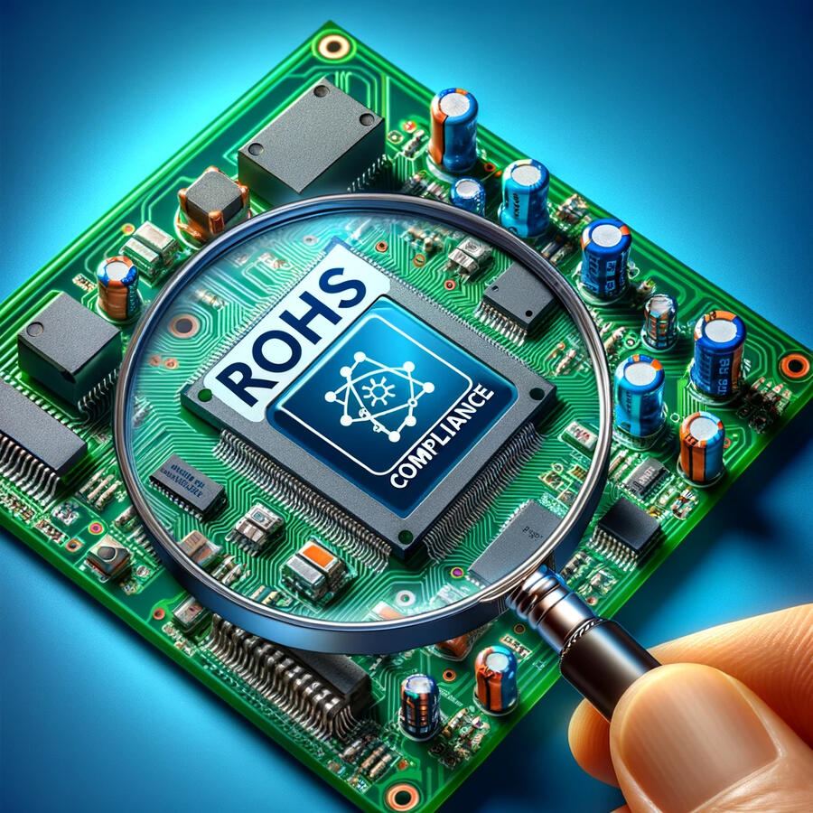
Understanding RoHS Compliance in PCB AssemblyIn the world of electronics manufacturing, particularly in Printed Circuit Boards (PCBs) assembly, RoHS compliance is not just a standard—it's a commitment to global responsibility and consumer safety. RoHS, which stands for Restriction of Hazardous Substances, is a piece of legislation enacted by the European Union that restricts the use of specific hazardous materials found in electrical and electronic products.The Essence of RoHS ComplianceRoHS compliance is crucial for companies that manufacture, sell, or distribute electronics in the EU, and it has become a de facto standard in many other parts of the world. The directive aims to protect the environment by ensuring that electronics products are free from substances that can pollute landfills and are dangerous to landfill workers. Additionally, it safeguards consumers from exposure to these substances in their daily lives.Substances Restricted by RoHSThe directive covers the restriction of the following ten substances:1. Lead (Pb)
2. Mercury (Hg)
3. Cadmium (Cd)
4. Hexavalent chromium (Cr(VI))
5. Polybrominated biphenyls (PBB)
6. Polybrominated diphenyl ethers (PBDE)
7. Bis(2-ethylhexyl) phthalate (DEHP)
8. Butyl benzyl phthalate (BBP)
9. Dibutyl phthalate (DBP)
10. Diisobutyl phthalate (DIBP)These substances are known to be harmful to both the environment and human health.The Impact on PCB AssemblyFor PCB assembly, RoHS compliance means that all components soldered onto the board must be free of these substances. This has led to significant changes in the industry, including the development of lead-free solders and the redesign of components to eliminate other RoHS substances.Lead-Free SolderOne of the most significant changes was the switch from traditional tin-lead solder to lead-free alternatives. Lead-free solders typically consist of a mixture of tin, copper, and other metals. This transition was not without challenges, as lead-free solders have different melting points and mechanical properties, which required adjustments in the PCB assembly process.Component SelectionComponents themselves must also be RoHS compliant. This means that manufacturers must source parts that do not contain any of the restricted substances. This can affect everything from capacitors to switches and connectors.Steps to Ensure RoHS Compliance1. Supplier Vetting: Establish a strict vetting process for suppliers to ensure that all components are RoHS compliant.2. Documentation: Maintain comprehensive records that demonstrate compliance for all parts used in PCB assembly.3. Process Adaptation: Adjust assembly processes to accommodate lead-free solders and other RoHS-compliant materials.4. Testing and Certification: Implement regular testing to ensure that products meet RoHS standards and obtain RoHS certification for products.5. Continuous Monitoring: Stay informed about any changes to RoHS regulations and adapt accordingly.Benefits of RoHS Compliance- Market Access: Compliance is mandatory for selling to the EU market and many others that have adopted similar standards.
- Environmental Responsibility: It demonstrates a commitment to reducing environmental impact.
- Consumer Safety: It ensures that products are safer for consumers to use.
- Brand Image: Compliance can enhance brand reputation as a responsible manufacturer.ConclusionRoHS compliance is a non-negotiable aspect of PCB assembly in today’s global electronics market. It requires a proactive approach to supplier selection, component sourcing, and manufacturing processes. By embracing RoHS standards, companies not only adhere to legal requirements but also contribute to a safer environment and public health, while positioning themselves as responsible and forward-thinking entities in the market.
Blog
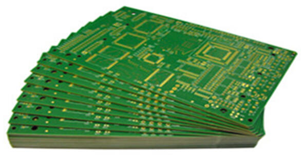
A Guide to PCB Material Selection
Understand Your Project Requirements: Start by thoroughly understanding your project's specifications and requirements. Consider factors like operating temperature, signal frequencies, and mechanical constraints. This will guide your material selection process.
Material Types: PCB materials come in various types, each with its own set of characteristics. The most common types include FR-4, FR-2, and high-frequency materials like PTFE (Teflon) and Rogers. FR-4 is a widely used, cost-effective option for general-purpose PCBs, while high-frequency materials are ideal for applications involving RF (radio frequency) signals.
Electrical Properties: Evaluate the electrical properties of the materials. Look at parameters such as dielectric constant (Dk), dissipation factor (Df), and impedance control. These properties affect signal integrity and overall performance.
Thermal Management: Consider the thermal properties of the material, especially if your project involves components that generate heat. Some materials have better thermal conductivity, helping dissipate heat efficiently.
Mechanical Strength: Assess the mechanical strength and rigidity of the material. If your project needs a flexible PCB, you might opt for materials like polyimide (PI) or flexible FR-4.
Cost and Availability: Budget constraints and material availability are practical factors to consider. While exotic materials may offer superior performance, they can be costly and less accessible.
PCB Layer Stackup: Determine the number of layers your PCB needs. High-density designs often require more layers, which can influence material choice.
Environmental Considerations: Think about the operating environment of your device. Some materials are more resistant to moisture, chemicals, and extreme temperatures than others.
Manufacturing Process: Consult with your PCB manufacturer. Different materials may require specific fabrication processes, which can impact cost and lead time.
Test Prototypes: Before committing to a large-scale production run, it's advisable to create prototypes using your chosen material to ensure it meets your project's requirements.
Benefits of Careful PCB Material Selection: Improved Signal Integrity: Choosing the right material can enhance signal transmission and reduce interference, critical for high-frequency applications. Reliability: Proper material selection can increase the lifespan of your product by ensuring it can withstand environmental stresses.Cost Efficiency: Selecting an appropriate material from the start can prevent costly design changes and rework.
Performance Optimization: Tailoring your material to your project's needs can lead to optimal electrical and thermal performance.In conclusion, PCB material selection is a pivotal step in electronics design. By understanding your project's requirements, considering material properties, and working closely with your manufacturer, you can make informed choices that lead to more reliable and cost-effective electronic products. Remember, the right material can be the foundation for a successful tech venture. Good luck with your PCB material selection process!
Blog
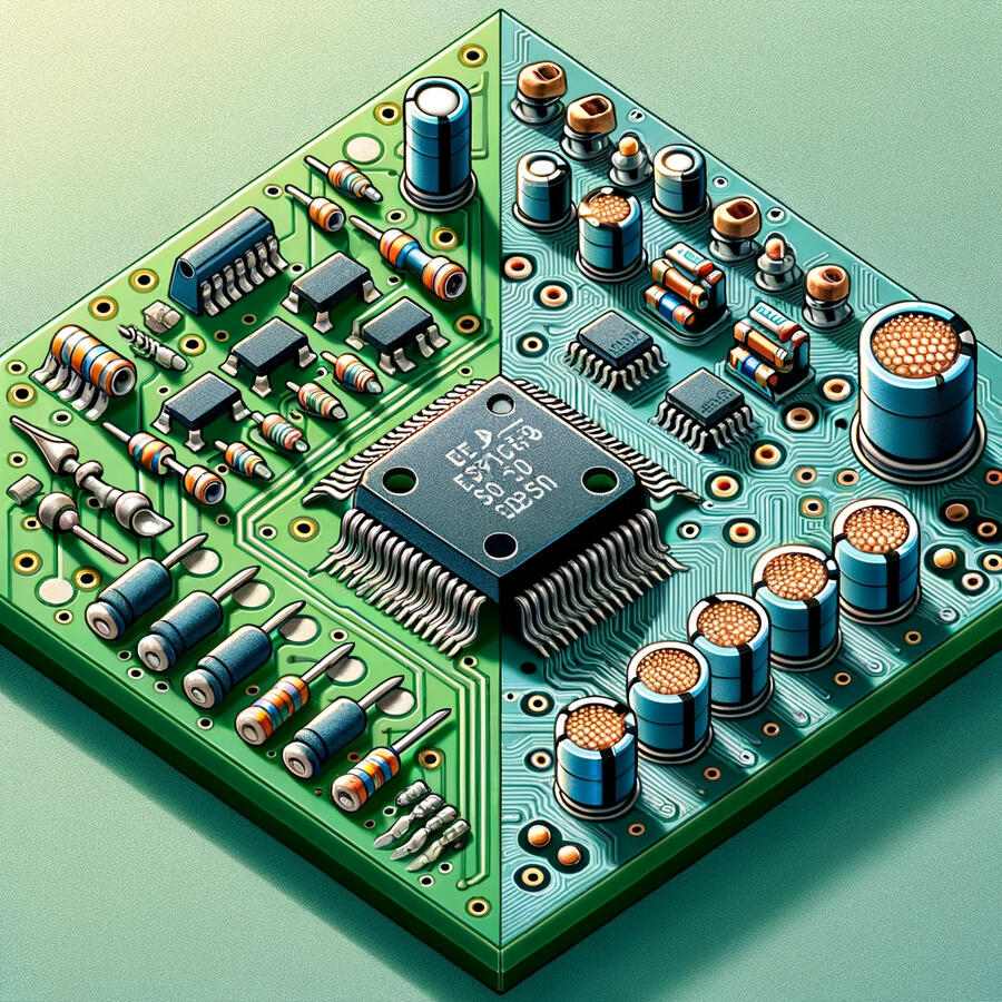
Choosing the Right PCB Component Placement: A Comparative Guide to SMT and THTIn the realm of Printed Circuit Boards (PCBs) assembly, the methodologies employed to affix components are pivotal to the board’s functionality and performance. Surface Mount Technology (SMT) and Through-Hole Technology (THT) stand as the two principal techniques in use today, each with its distinctive attributes and implications for PCB design. Here's an evaluative guide that will assist you in determining the most suitable component attachment method for your PCB design.Surface Mount Technology (SMT) offers a modern approach to component placement, boasting several advantages:- SMT components, known for their diminutive stature, allow for a denser component arrangement on the PCB which is a critical factor for sophisticated, high-density designs.
- The compatibility of SMT components, with automated pick-and-place machinery, streamlines the assembly process which trims down both time and cost.
- With their compact size, SMT components reduce the distance electrical signals must traverse, thus enhancing the performance, a benefit that becomes increasingly apparent in high-frequency applications.
- When it comes to mass production, the economies of scale favor SMT, thanks to the lower labor costs and heightened production throughput, which together contribute to its cost-effectiveness.However, SMT is not without its limitations:- SMT may falter in high-power scenarios or situations where mechanical stress is prominent, as the smaller components are less robust in such conditions.
- Due to their size, replacing or reworking SMT components is often a delicate and challenging task.The domains where SMT reigns supreme include compact electronic devices such as smartphones, laptops, and the burgeoning field of IoT devices, where space is at a premium and performance is key.On the other end of the spectrum, Through-Hole Technology (THT) presents a more traditional technique with its own set of strengths:- The leads of THT components penetrate the PCB, creating sturdy mechanical bonds, which is particularly advantageous for components that must endure heavy usage or high-power demands.
- THT components can be effortlessly reworked or replaced, making this technology a favored choice during the prototyping phase or for small-scale production endeavors.
- THT's robust connections lend a hand in ensuring reliability, an aspect critically important in products destined for high-stress environments or those that require a significant degree of durability.THT, however, comes with its own disadvantages:- The larger size of THT components necessitates bigger PCBs, which can be a drawback when trying to minimize the footprint of the electronic device.
- THT assembly typically involves more manual labor, which can inflate production costs and may not be conducive to scaling.
- The manual processes associated with THT result in slower production times compared to the more automated SMT.THT finds its niche in sectors where reliability and durability are non-negotiable, such as in industrial electronics, aerospace, and military technology.When it comes to choosing the right component determination method for PCB design, several factors come into play:- The intricacy of the PCB design often dictates the choice, with SMT being the preferred option for complex, space-constrained boards.
- The size and type of the components are also critical considerations; smaller, passive components are typically mounted with SMT, while larger or high-power components may necessitate THT.
- Manufacturing volume has a direct impact on cost-efficiency, with SMT being more economical for large-scale productions, whereas THT may be more cost-effective for smaller runs.
- Durability requirements must also be weighed; products that are subject to rough handling or harsh conditions are better served by the robustness of THT.
- During the prototyping and testing phase, the flexibility of THT is beneficial, but transitioning to SMT during full-scale production can optimize efficiency.
- Lastly, cost considerations should not be overlooked; while SMT may demand higher initial setup costs, the long-term savings in automation and material costs can offset the increased labor costs associated with THT.Selecting between SMT and THT is a decision that should align with the PCB design’s demands and the intended application of the final product. Often, the most effective approach may involve leveraging both technologies to harness their respective advantages, ensuring that the end result is both high-performing and cost-efficient. This comparative analysis aims to provide clarity and direction for designers and engineers as they navigate the complexities of PCB design and assembly.
Blog

Common Mistakes in PCB Design and How to Avoid ThemPrinted Circuit Boards (PCBs) are the unsung heroes that power our devices. From smartphones to spacecraft, PCBs are at the heart of modern electronics. However, even seasoned engineers can fall into the trap of common PCB design mistakes. In this article, we'll explore these pitfalls and provide actionable steps on how to steer clear of them.Mistake 1: Inadequate PlanningA PCB design without a solid plan is like a ship without a captain. To avoid this, start with a clear project plan. Understand the project's requirements, components needed, and expected performance. Create a checklist and timeline to keep your project on track.Mistake 2: Insufficient Power ConsiderationOne of the most critical aspects of PCB design is ensuring it can handle the required voltage and current without overheating. Calculate power requirements meticulously and employ appropriate power distribution techniques such as ground planes and power planes.Mistake 3: Poor Component PlacementEffective component placement can make or break a PCB design. Group related components, minimize signal path lengths, and follow best practices for component orientation. Utilize PCB layout software for optimal component placement.Mistake 4: Inadequate Signal Integrity AnalysisNeglecting signal integrity analysis can lead to signal quality issues such as reflections, crosstalk, and impedance mismatches. Perform this analysis early in the design phase and employ termination techniques and controlled impedance traces as needed.Mistake 5: Ignoring Thermal ManagementHeat is the enemy of electronics. Overlook thermal management, and your PCB could fry. Ensure proper spacing for heat sinks and components that generate heat. Leverage thermal vias and copper pours to dissipate heat effectively.Mistake 6: Neglecting EMI/EMC ComplianceElectromagnetic interference (EMI) and electromagnetic compatibility (EMC) are crucial considerations. Design with these in mind by adhering to guidelines, using proper grounding techniques, and implementing shielding if necessary.Mistake 7: Skipping Design Rule Check (DRC)Running a Design Rule Check (DRC) is non-negotiable. This step helps catch errors like spacing violations and trace width issues. It's a small effort that pays big dividends in error prevention.Mistake 8: Not Testing and PrototypingDon't jump straight from design to mass production. Testing and prototyping are essential steps. Ensure your design works as expected and iterate as necessary to uncover and fix any issues.Mistake 9: Overlooking DocumentationComprehensive documentation is often underestimated. Maintain detailed records throughout the design process, including schematics, PCB layout files, bill of materials (BOM), and assembly instructions. This documentation is your lifeline for troubleshooting and future revisions.Mistake 10: Rushing the DesignFinally, patience is key. Rushing through the PCB design process is a recipe for disaster. Allocate enough time for research, design, testing, and revisions. Quality PCB design demands a meticulous approach.Final Thoughts
In the field of PCB design, avoiding common mistakes is crucial for success. Engineers and designers often encounter pitfalls like inadequate planning, insufficient power considerations, suboptimal component placement, and insufficient attention to thermal management. Signal integrity analysis and compliance with EMI/EMC standards are essential, as is conducting a thorough Design Rule Check (DRC) and robust testing and prototyping. Detailed documentation and patience play pivotal roles. By adhering to these principles, PCB designs can be error-free and reliable, in harmony with the meticulous standards of the tech industry, which is vital for those navigating the dynamic landscape of technology.
Blog
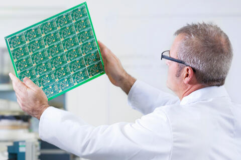
Overview of the Different Types of Printed Circuit Boards (PCBs)IntroductionIn today's technology-driven world, Printed Circuit Boards (PCBs) are the linchpin that holds most electronic devices together. They're in your smartphones, your car's navigation system, and even in life-critical medical devices. Hence, it's essential for anyone in the tech industry to have a solid grasp of the various types of PCBs, their applications, and benefits. Let's dive in.Single-Sided PCBsStarting with the basics, single-sided PCBs are the most straightforward type of PCB you'll encounter. These boards consist of a single layer of substrate, usually made of fiberglass, with conductive tracks etched onto one side. Due to their simplicity, they are commonly found in consumer electronics like radios and calculators, as well as in basic control systems. Their primary advantages lie in their low cost and ease of manufacture. So, if you're working on a simple project or prototype, opting for a single-sided PCB is a practical, cost-effective choice.Double-Sided PCBsTaking it a step further, we have double-sided PCBs. These boards feature conductive tracks on both sides, which allows them to house more complex circuits. You'll often find them in industrial controls, automotive systems, and HVAC units. Compared to their single-sided counterparts, double-sided PCBs offer increased circuit density and more flexible design options. Therefore, for projects that require a moderate level of complexity but are still budget-sensitive, a double-sided PCB can be an excellent compromise.Multilayer PCBsFor those dealing with extremely complex circuits, multilayer PCBs are the gold standard. These boards consist of three or more conductive layers, separated by insulating materials. They are the go-to choice for high-end applications like computers, servers, medical imaging devices, and satellite systems. With high circuit density and the capability for high-speed circuitry, multilayer PCBs offer unmatched performance and reliability. If you're developing technology that requires advanced capabilities, multilayer PCBs are likely your best bet.Rigid, Flexible, and Flex-Rigid PCBsNow, let's talk about form factors. Rigid PCBs are your conventional, inflexible boards commonly used in various consumer electronics. On the other end of the spectrum, flexible PCBs are crafted from pliable plastic substrates and are ideal for applications where the board needs to bend or fold. Then, we have flex-rigid PCBs, which offer the best of both worlds. These boards are commonly used in advanced electronics that require a combination of flexibility and rigidity. The form factor you choose should align with the specific needs of your device.Specialized PCBsFinally, for those who require something more specialized, there are aluminum-backed PCBs and high-frequency PCBs. Aluminum-backed PCBs are excellent for heat dissipation, making them ideal for LED lighting and power supplies. High-frequency PCBs, on the other hand, are designed for use in radio frequency (RF), microwave, and millimeter-wave circuits and require specialized materials for their construction. If you find yourself in need of a specialized PCB, it's crucial to consult a manufacturer with expertise in that area.Final ThoughtsArmed with this knowledge, you're well-equipped to make informed decisions about the type of PCB that best suits your project's needs. Whether you're developing a simple gadget or a cutting-edge technological marvel, your choice of PCB plays a critical role in your project's success. Keep this guide in mind, and you'll be well on your way to optimizing your tech ventures for both performance and cost-effectiveness.
Blog
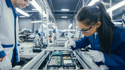
Basics of PCB Assembly: An Introduction for Beginners
In the technologically driven world we reside in, the demand for compact, efficient, and robust electronic devices is ever-increasing. At the heart of these devices lies a crucial component known as the Printed Circuit Board (PCB). The journey of transforming a PCB from a bare board to a functional one filled with electronic components is known as PCB Assembly. This process is fundamental to the creation of a vast array of electronic gadgets we rely on daily.In this introductory guide, we'll dive into the basics of PCB Assembly, shedding light on the core steps involved, the types of assembly techniques used, and why this process is pivotal in electronics manufacturing.Core Steps Involved in PCB Assembly
Design and Testing:
Before the assembly process kicks off, a thorough design of the circuit is crucial. Utilizing specialized software, engineers design the circuit layout, ensuring optimal performance and functionality. Once the design is finalized, it's tested for any potential flaws or improvements.Preparation of the PCB:
The bare PCB is prepared by cleaning it to ensure there are no contaminants that could interfere with the assembly process. This step lays the foundation for a successful assembly.Placement of Electronic Components:
Once cleaned, the electronic components are placed on the PCB. This can be done manually or through automated machines, with the latter being the most common in professional settings due to its accuracy and efficiency.Soldering:
Soldering solidifies the connection between the components and the PCB. Two primary methods are used: Surface Mount Technology (SMT) and Through-Hole Technology (THT).Inspection and Quality Control:
Post assembly, it's imperative to inspect the PCB to ensure all components are correctly placed and soldered, with no short or open circuits.Testing:
Functional testing is conducted to ensure the assembled PCB operates as intended.Assembly Techniques:
Surface Mount Technology (SMT):
SMT is a modern assembly technique where components are mounted directly onto the surface of the PCB, allowing for more components to be placed on both sides of the board.Through-Hole Technology (THT):
THT is a traditional method where components' leads are threaded through holes drilled in the PCB. Although it provides strong mechanical bonds, it's gradually being replaced by SMT due to the latter's space efficiency and cost-effectiveness.The Significance of PCB Assembly:
PCB Assembly is a linchpin in electronics manufacturing, bridging the gap between a conceptual design and a tangible, operational device. By understanding the basics of PCB Assembly, not only can one appreciate the complexities and the artistry involved in electronics manufacturing, but also make informed decisions when embarking on a PCB project.In conclusion, the world of PCB Assembly is vast and intricate. The journey from a bare board to a fully functional circuit is a fascinating process, central to bringing electronic innovations to life. Whether you are a hobbyist, a student, or a professional in the electronics field, having a solid grasp of PCB Assembly basics is indispensable.
Blog
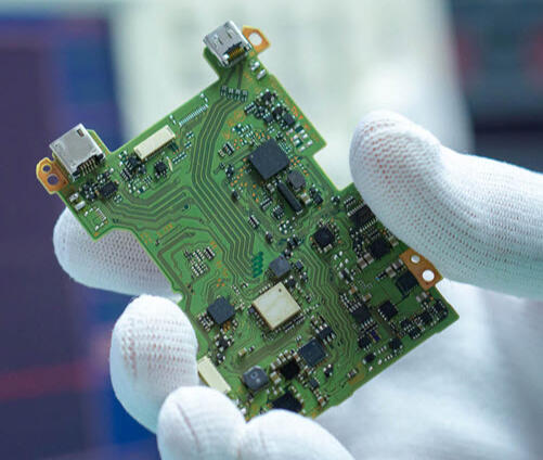
What is a Printed Circuit Board (PCB)?
The Printed Circuit Board (PCB) acts as the linchpin holding various electronic components together in a meticulously designed arrangement. Its significance cannot be understated as it's the platform where different electronic components come together to perform harmonized operations.At its core, a Printed Circuit Board is a thin plate made of insulating material, which is often fiberglass or plastic. Onto this plate, conductive pathways or tracks are printed or etched, forming a sophisticated network of electrical circuits. These circuits interlink various electronic components such as transistors, resistors, and capacitors, which are meticulously soldered onto the board.Design Precision: The design of a PCB is a meticulous process that demands a high degree of precision. Engineers employ specialized software to layout the circuit design, ensuring optimal performance and avoiding any potential short-circuits. This digital blueprint is then used to manufacture the PCB, ensuring each component and circuit trace is placed with pinpoint accuracy.Mass Production: The advent of PCBs has revolutionized mass production of electronic devices. Traditional wire-wrapped or point-to-point constructed circuits were not only bulky but also inconsistent in performance. PCBs ushered in a new era of compact, reliable, and replicable electronic circuit design, which is instrumental in the mass production of electronics, thereby driving down costs significantly.Troubleshooting and Repair: The organized layout of a PCB makes troubleshooting and repairs more straightforward. With a well-designed PCB, identifying and rectifying faults becomes a systematic and less daunting task. Moreover, the standardization in PCB design also facilitates easier replacement or upgrading of components.Durability and Reliability: PCBs are known for their durability and reliability. The absence of loose connections and wires, and the fixed components contribute to the longevity and robust performance of electronics built with PCBs.Performance Enhancement: The precise design and organized layout of a PCB contribute to enhanced performance. The minimized electrical noise, for instance, ensures that the circuit performs with better accuracy and reliability.Environmental Footprint: In comparison to older circuitry methods, PCBs are more environmentally friendly. They require fewer resources and generate less waste, embodying a step towards more sustainable electronic manufacturing.Harnessing the potential of PCBs is fundamental in driving innovation in the electronic landscape. Whether it's a simple gadget or a complex piece of industrial equipment, the Printed Circuit Board is at the heart of ensuring seamless operation and advancing the frontier of technological evolution. The utility and advantages of PCBs underscore why they are the cornerstone of modern electronic design and manufacturing.
Press Release

Ansync Labs Unveils Sacramento PCB Assembly
El Dorado Hills, CA – October 21, 2023– Ansync Labs is excited to announce the launch of its subsidiary, Sacramento PCB Assembly. Offering a comprehensive range of printed circuit board (PCB) assembly services, this new venture is set to redefine industry standards. By harmonizing state-of-the-art technology with skilled craftsmanship, Sacramento PCB Assembly ensures exceptional precision and quality at every phase of the assembly process.Sacramento PCB Assembly meticulously orchestrates each project from initial part procurement to final shipping, adhering to an approved Bill of Materials (BOM) while leveraging advanced inspection techniques like 3D Automated Optical Inspection (AOI) and X-Ray technology. This stringent quality control results in meticulously assembled PCBs, ready for immediate integration into client projects.Discover a world of superior electronics manufacturing by visiting sacramentopcbassembly.com. Engage with a team dedicated to delivering industry-leading solutions that meet the unique needs of every project.For media inquiries:
Rich Foreman
Chief Marketing Officer
916.692.9706
rich.foreman@ansyc.comAbout Ansync Labs:
Situated in Northern California, Ansync Labs is a design-for-manufacture firm embracing a multidisciplinary approach for solution development and product realization. Our team of engineers, supported by an in-house machine shop and electronics assembly line, is dedicated to delivering practical solutions in motors and automation, medical, and IoT devices, aiming to create a positive impact.About Sacramento PCB Assembly:
Sacramento PCB Assembly provides end-to-end printed circuit board assembly services, blending cutting-edge technology with expert craftsmanship for precision and quality. Services include planning based on an approved Bill of Materials (BOM), solder paste application, automated and manual component placement, varied soldering methods, and advanced inspection techniques like 3D Automated Optical Inspection (AOI) and X-Ray technology. The outcome is a thoroughly assembled PCB, ready for immediate integration into your projects.
About Us
Sacramento PCB Assembly offers a comprehensive printed circuit board assembly service that covers every aspect of the process, from initial part procurement to final shipping. Utilizing a blend of cutting-edge technology and skilled craftsmanship, we ensure precision and quality at every step. The service includes meticulous planning based on an approved Bill of Materials (BOM), precise solder paste application, automated and manual component placement, and a variety of soldering methods tailored to each project's unique requirements. Advanced inspection techniques, such as [3D Automated Optical Inspection AOI and X-Ray technology, are employed to guarantee the highest quality standards. The end result is a meticulously assembled PCB, cleaned and packaged with industry-standard materials, ready for immediate integration into your projects.
5175 Hillsdale Cir. Suite 150
El Dorado Hills, California 95762
Sacramento PCB Assembly is a division of Ansync Labs headquartered in El Dorado Hills, California. We serve the Northern California Region including Sacramento, Elk Grove, Roseville, Folsom, Rancho Cordova, Davis, Woodland, Citrus Heights, Rocklin, West Sacramento, Auburn, Lincoln, San Francisco, Oakland, San Jose, Berkeley, Palo Alto, Mountain View, Sunnyvale, Santa Clara, Redwood City, Menlo Park, Cupertino, Fremont, Hayward, San Mateo, Concord, Vallejo, Fairfield, Richmond, Daly City, San Rafael, Petaluma, Novato, Santa Rosa, Napa, Livermore, Pleasanton, Walnut Creek, Alameda, San Leandro, and San Ramon.
To learn more about our X-Ray Inspection Services visit: SacramentoXrayInspection.com
To learn more about our Prototype Development visit: SacramentoPrototypeShop.com